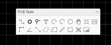
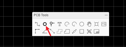
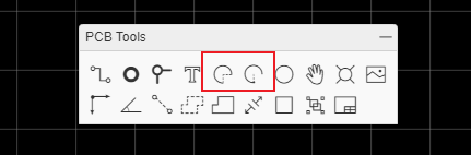
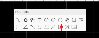
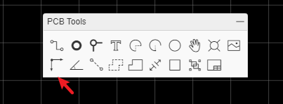
PCB Tools
PCB tools provide many function to fulfill your PCB design requirement. Such as: Track, Pad, Via, Text, Arc, Circle, Move, Hole, Image, Canvas Origin, Connect Pad to Pad, Copper Area, Solid Region, Measure/Dimension, Rect, Group/Ungroup. etc.
Track
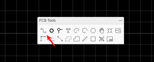
In the schematic editor, we use Wire or the W Hotkey to connect Pins, in a similar way in the PCB editor, we use Track to connect Pads. Track allows you to draw PCB tracks and can be found on the PCB Tools palette or using the W Hotkey (not T: see above!).
When a track is selected, you can find its Length attribute in the right panel. 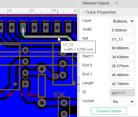
If you want to create solder mask for the track, you can click the "Expose Copper" button at the right-hand property panel.
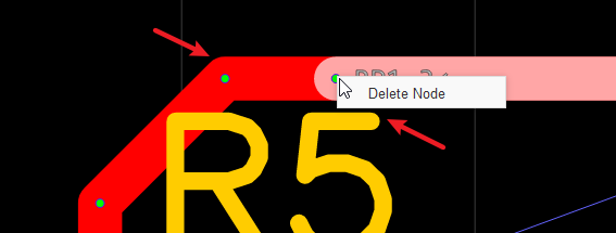
When click the track, you will see the nodes, you can drag it or right-click delete it.
when select the point to point separated tracks, you can convert them as Solid Region or continus track at right-click menu.
The more information of routing, please refer at PCB: Route Tracks
Pad
You can add pads using the Pads button from the Footprint Tools palette or using the P hotkey.
After selecting one of the pads, you can view and adjust its attributes in the right hand Properties panel.

Number: Remembering the pin numbers you set in the schematic symbol in your Schematic Lib: to connect those schematic symbol pins to the pads in your PCB footprint, the pad numbers you set here in the Footprint footprint must be the same.
Shape: Round , Rectangular , Oval and Polygon.
EasyEDA supports four shapes: Round , Rectangular , OVAL and POLYGON.
OVALPAD will give your more space.POLYGONPAD will let you to create some strange pad.
Like in the image below, you can edit the PADs points when you select a POLYGON PAD 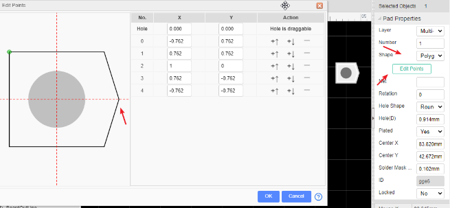
Layer: If the pads are part of a SMD footprint, you can set it to Top layer or Bottom layer. For through hole components you should set it to Multi-Layer. If it setting as mult-layer, it will connect with all copper layers.
Net: You don't need to enter anything here because at present this footprint is not connected to anything in a circuit.
Width and Height: When the shape is set to Round, Width will equal Height.
Rotation: Here you can set the Pad's rotation as you want.
Hole(D): This is the drill hole diameter for a through hole pad. For a SMD Pad, set its layer to TopLayer or BottomLayer.
Hole Shape: Round and Slot. When it is set as a slot, the Gerber is generated through the stitching of multiple drill holes in the corresponding position. If your hole is round, please do not set it as a slot, so as to avoid the overlapping error of holes during the production of DFM detection.
Center-X and Center-Y: using these two attributes, you can set the pad's position with more precision, compared to using the mouse.
Plated: Yes or No. When you set it as No, this pad Inner wall do not metallization.
Paste Mask Expansion: For single layer pad. This property affects the size of the tin area on the plate of the steel mesh. If you want to set a pad that is not open in the steel mesh, you can set the value to be negative, which is usually larger than the diagonal of the pad.
Solder Mask Expansion: This property affects the size of the green oil area cover on the pad. If you want to set a pad not open covered with green oil, you can set the value to be negative, the value is usually set larger than the diagonal of the pad.
And you can select a track/Solid Region, right-click it and convert to a pad. 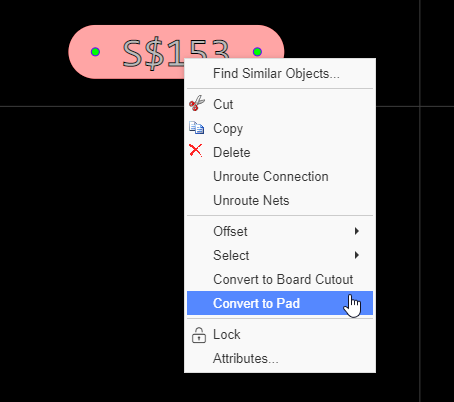
Via
When you want to lay a multilayer PCB, you need to add Vias for nets getting through layer and layer. 
Place a Via on a Track
When placing a via on a track, the track will be cut to two segments, and the via net will follow track's net. Placing two vias on a tracks, you will get three segments, then you can change one segment to other layer id, or remove one of them. 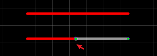
Place Multiple Vias
Click the copper area outline, click the "Add/Remove Vias" button. this feature needs the same net copper areas on two and more layers in the same time, the cross area will add the vias. 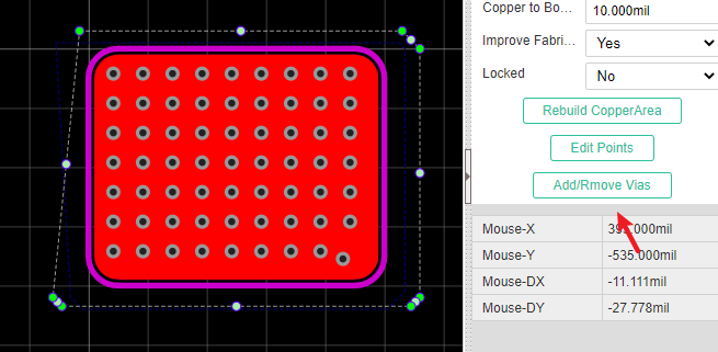
Notice:
- EasyEDA only support the through via for all layers, doesn't support the buried/blind via.
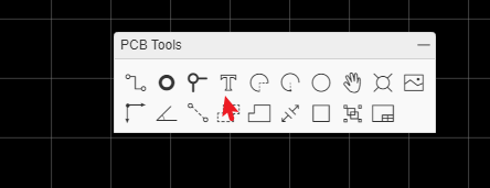
Text
You can add more fonts from your computer or download free fonts: http://www.fontspace.com/.
if you need Japanese or Korean you can use Google Noto fonts
The editor including fonts are: (NotoSansCJKsc-DemiLight)[https://github.com/googlefonts/noto-cjk/blob/main/Sans/OTF/SimplifiedChinese/NotoSansCJKsc-DemiLight.otf] (NotoSerifCJKsc-Medium)[https://github.com/googlefonts/noto-cjk/blob/main/Serif/OTF/SimplifiedChinese/NotoSerifCJKsc-Medium.otf]
Select the text, then you can find a Font-family attribute on the right panel like in the image below. 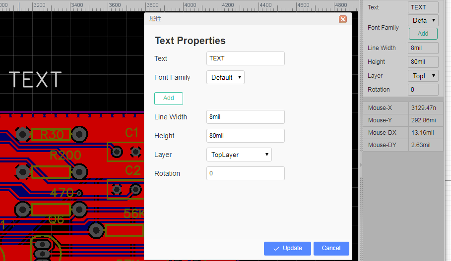
Click the add button, then choose the font, the font file must be ttf or otf. 
So you can add any fonts by yourself. EasyEDA doesn't cache the font on our server, so if you close the editor, you need to add the font again by yourself.
Note: If you use the other font, the LineWidth attribute is useless, because it will be automatically set by changing the Height.
Arc
You can draw many Arcs with different sizes, it's easy to create a pretty cool PCB as you like.
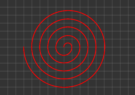
EasyEDA provides two Arc tools:
Start point fixed, you can change the end point position and radius.
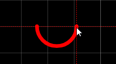
Center point fixed, you can change the radius.
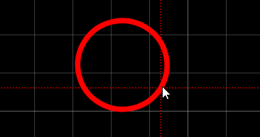
Select the arc, you can change the arc type at property panel, different arc type has different drag behavior. 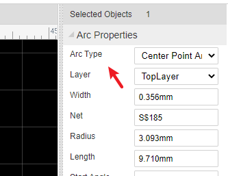
Circle
You can draw a circle in PCB. If you want to draw a circle at TopLayer or BottomLayer, please use Arc.
Move
This option is same as schematic's drag. 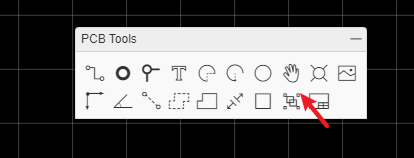
Hole
There were lots of users that didn't know how to use PAD or VIA as a HOLE, they asked EasyEDA for help, so EasyEDA added a HOLE TOOL in the PCB toolbar. 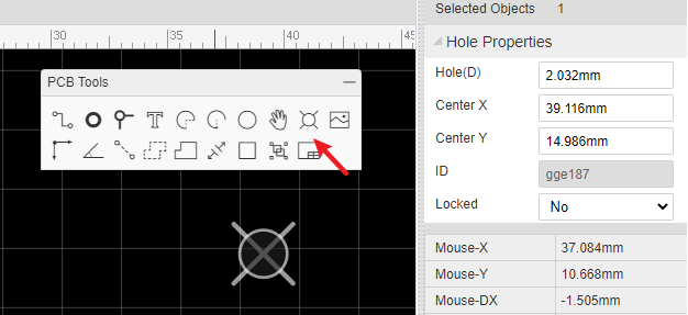
And if you want to create the slot hole, you can use solid region(Type: NPTH), or route a track, and then right-click the "Convert to NPTH" menu.
Image
On PCB and Footprint editor, there is a nice feature on the PCB Tools bar.
After clicking on the image icon, you will see the Insert Image window as below. 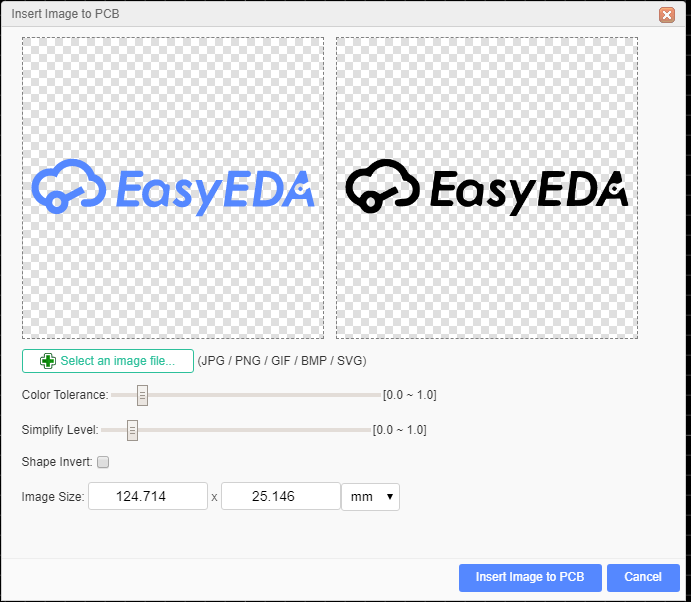
In this dialog, you can choose your favorite image, EasyEDA support JPG, BMP, PNG, GIF, and SVG. Unlike some other EDA tools which only support a Monochrome Bitmap image, EasyEDA supports full color, but Monochrome Bitmap is welcome.
You can adjust the color tolerance, simplify level and reset the image size there.
And you can select shape invert.
The image will be inserted to the active layer, if it is not right, you can change the attribute. Such as TopSilkLayer. 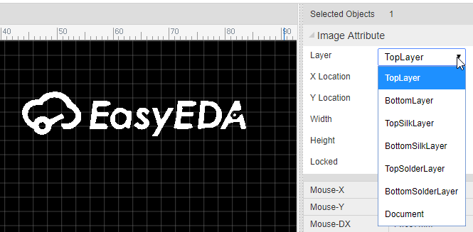
Canvas Origin
This option is the same as schematic's Canvas Origin.
Protractor
We provide a protractor for PCB tools. 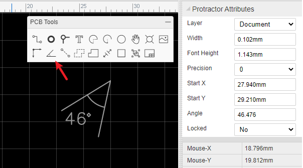
Connect Pad to Pad
When creating a PCB without a Schematic, none of the pads on the Footprints have nets connecting them so there will be no ratlines.
Rather than try to track the pads from scratch, it is a good idea to connect them up by hand first using Connect Pad to Pad from the PCB Tools palette. This will help you to remember to track the pads correctly with fewer mistakes.
You could also do this by setting net names for all the pads: if the two pads are given the same net name then EasyEDA will understand that they are connected together and will automatically create a ratline between them. 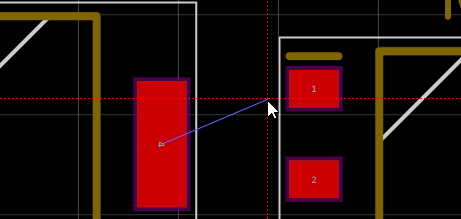
Or you can set these two pads with the same net name at the right panel Pad Properties after you click the pad.
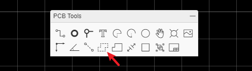
Copper Area
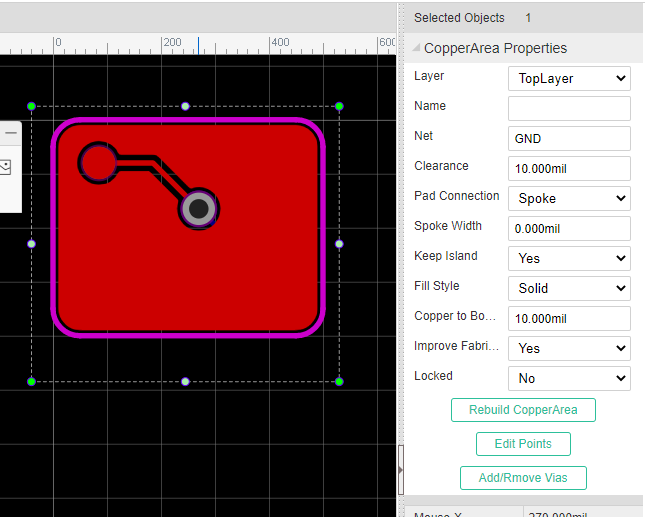
Sometimes you will want to fill in or flood an area with copper. Usually this copper area will be connected to a net such as GND or a supply rail. You can draw the outline of a flood using the Copper Area button from the PCB Tools palette.
When selecting a copper area, you can find its attributes from the right hand Properties panels.
The more information please refer at PCB: Copper Pour
Solid Region
EasyEDA has added a new tool Solid Region for PCB design
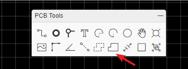
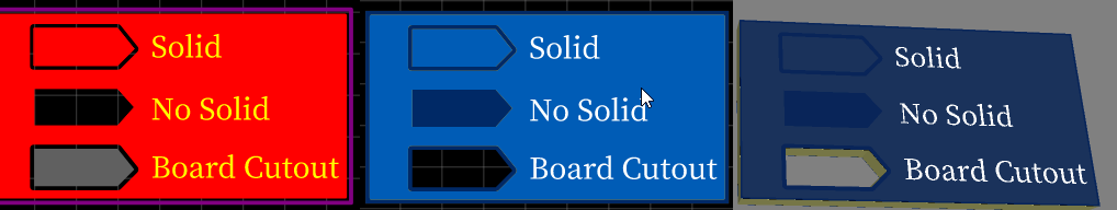
This is a very useful, quick way to connect Pads. You can draw a Solid Region to include all of these pads with same net name, then set the region to the same net name as the pads. It is like Copper Area but easier to use for small areas. To use Solid Region like this, set the Type attribute (in the right hand Properties panel) to Solid.
The more information please refer at PCB: Solid Region
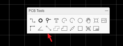
Measure/Dimension
Making and adding measurements is useful in PCB design. EasyEDA provides two methods to do this.
Dimension tool in the PCB Tools palette: This tool can show three units on the canvas, milliliter, inch and millimeter.
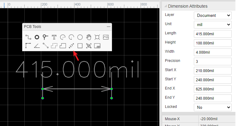 When you click one side of the dimension on the PCB, you can drag it for any directions or change its length.
Measure a distance using Hotkey M, Or Via: Top Menu > Edit > Measure Distance, then click the two points which you would like to measure.
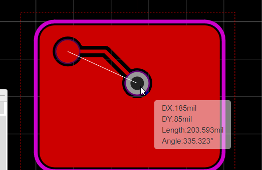 Tips: - It's unit follows canvas's units. - You can disable the snap option to measure at the canvas property panel.
Rect
It looks like a Solid Region, but it can't be set Nets and you can't set the Layer as NTPH.
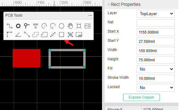
The rect doesn't rotate, you can change its width and height.
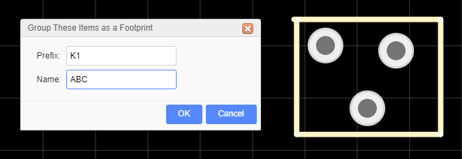
Group/Ungroup
Just like Group/Ungroup in the Schematic Editor can be used to create a schematic lib symbol, you can use Group/Ungroup from the PCB Tools palette to create a Footprint footprint in the PCB editor.
For example, place Tracks and Pads on the canvas, then select all of them and click Group/Ungroup to group them like as a footprint in the image below:
Notice:
- Before ungroup the footprint, please change it's layer to top layer first, because of the footprint after grouping will at top layer.
- The grouped footprint doesn't support Import Changes, it will be removed if you Import Changes.