EasyEDA Std PCB FAQ
PCB
How to solve the PCB very slow issue
Details
Because of v6.3 add two features:
- All objects support show the ratlines which are containing nets;
- Solve bottom layer pads will cover top copper issue. These features will make editor slower than before.
There are some methods to try to improve:
- Via Tools - Design Rule, disable real-time DRC
- Via Settings - PCB settings, disable Add Teardrop Automatically
- Via Settings - PCB settings, disable Net Highlighting While Coursor Hover the Track
- Via Settings - PCB settings, disable The Track's Routing Follows Component's Rotation
- Via Settings - PCB settings, disable Rebuild Plane Automatically, and using copper area instead of inner plane layer
- Via Settings - PCB settings, set Canvas Zoom Effect as Speed Priority
- Hide ratline layer before move footprints at PCB
- Check footprints which have a lot pad's, and the pads are polygon type, please modify them as Retangle or Oval
- Suggest PCB doesn't over 300 footprints, Pads and Vias no more than 1500
How to change the Units of PCB from mil to mm or inch.
Details
There is an option for that in PCB canvas attributes: 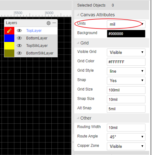
How to pick and move the components on the PCB canvas quickly.
Details
Before routing the PCB, the components need to be positioned in suitable places on the PCB. In the PCB Editor, it can sometimes be quite difficult to select components by clicking on the silkscreen outline or the pads. To select and move them more easily, please use drag mode (Hot Key D) or click the Move icon in the PCB Tools toolbar: 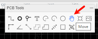
How to add test point in schematic or PCB?
Details
Schematic: You can place a single pin connector from Commonly Library, and then update its footprint.
PCB: You can place a top/bottom layer pad , and then route it with track.
Can I create a PCB without creating schematic?
How to add more fonts for PCB.
Details
You can refer to Text of PCB section.
How to insert an Image/Logo to PCB.
Details
You can refer to Image of PCB section.
How to insert a DXF as board outline.
Details
You can refer to Import DXF File of Import section.
How to create non rectangular pcb outline such as round?
Details
You can import a DXF file for the board outline. For a round board outline, you can use an arc to do that, you just need to change to the board outline layer, then draw 1 arc like in the image below (need to adjust a bit later), you can use lines and arcs to create complex board outlines.
How to measure dimensions on a PCB.
How to add more layers.
Details
Click the layer options button, then tick the extra layers in the dialog that opens. https://docs.easyeda.com/en/PCB/Layers-Tool/index.html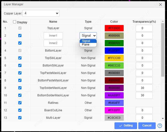
How to add solder mask aperture.
Details
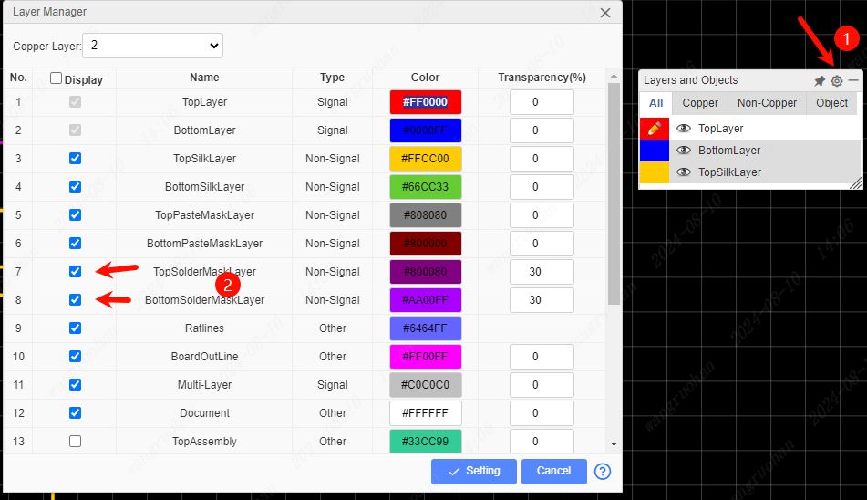
It is possible to get boards with the copper exposed so that you can apply a layer of solder over those tracks to further increase their current carrying capacity. In this case, you need to add solder mask over a copper (copper area, track, solid region). EasyEDA will add solder mask for pads automatically. Sometimes however, you may need to add an aperture in the solder mask to expose and area of copper.
First, add a top or bottom solder mask layer, as required.
Next, draw a region in the solder mask layer over a copper item as illustrated in the image below. This in effect draws an aperture in the solder mask so that the copper item inside the region, in this case the track, will be not be covered by the green film of solder mask.
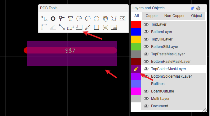
A common mistake is to just draw a solder mask, without a copper area, like the track pointed to by the yellow arrow. That is incorrect and does not produce the desired result.
Or you can click the track, and then click the Expose Copper button at the right-hand panel. 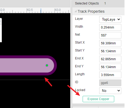
How do I set the dimensions of my PCB in the layout?
Details
PCB's dimension/size depends on the board outline, you can create your board outline, please refer to Board Outline of the PCB section.
My PCB is complex, how can I be sure that I have routed all of the tracks?
Details
Please refer to Design Manager of PCB section.
I need to start my layout again, how can I remove all of the tracks?
Details
You can use "Menu - Route - Unroute All" and "Menu - Edit - Global Delete".
How to put a component on the bottom layer?
Details
There are two ways to do this.
- If your active layer is the bottom layer, then every component you place will be placed on the bottom layer automatically.
- You can place a component then select it and change its layer attribute to
Bottom layerin the right hand panel.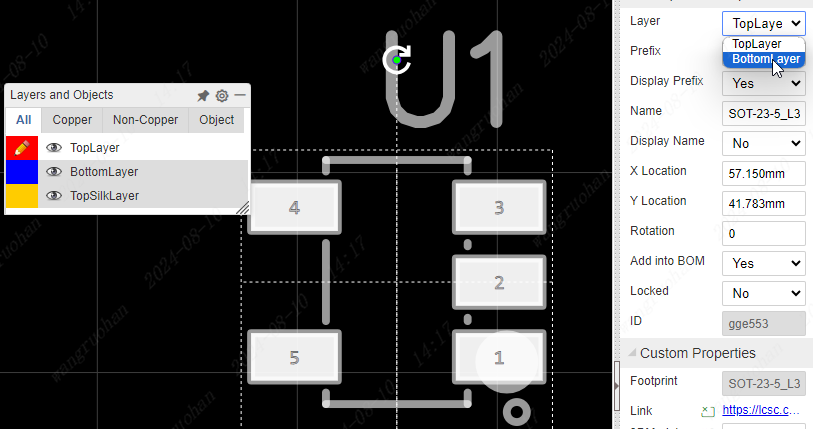
How to panelize the PCB
Details
Please refer at PCB: Panelize
What does Warning copper area do not allow self intersection
Details
Please refer at Forum: What does Warning copper area do not allow self intersection
Why can't the pad number be directly seen in the EasyEDA Std PCB?
Details
Because the system is invisible by default, it can only display the network, or view it in the right property bar, so we need to open it in the pcb setting 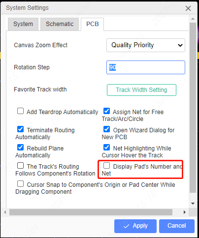
How to batch modify pad network in pcb?
Details
First select the pads you want to modify in bulk, click the right mouse button and select ‘Find Similar Objects’. 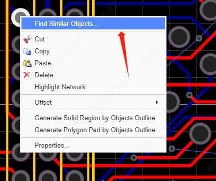
And then look up the rule and delete the network here. You can customize the shape of the pad object you want to batch select according to your needs, etc. 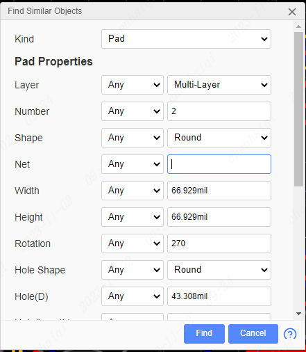
After clicking "find", it will help you find all the pads that match the requirements, and then modify the network you want in the properties bar on the right. 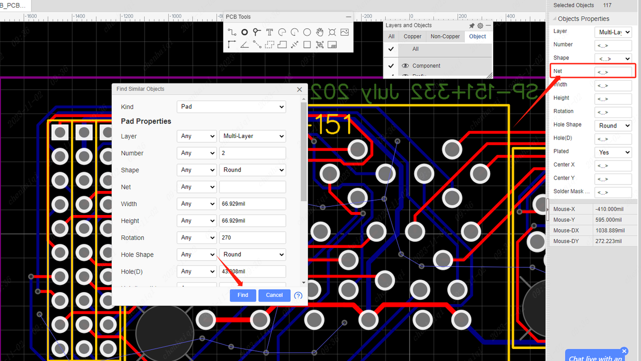
How to change the line width?
Details
First way: After the wiring is done, select the wire and change the width in the properties bar "Width" on the right. 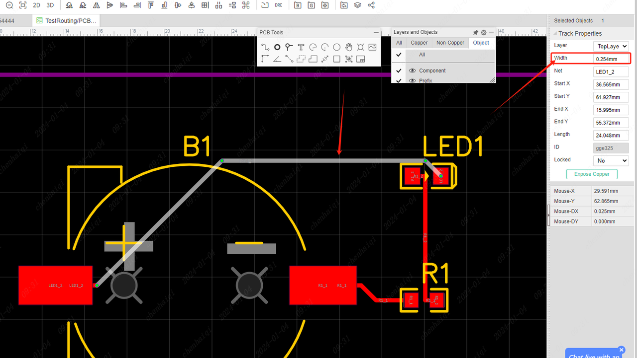
The second method: in the process of wiring, first pull out a wire, and then press the "tab" key, a prompt box will pop up to change the wire width. 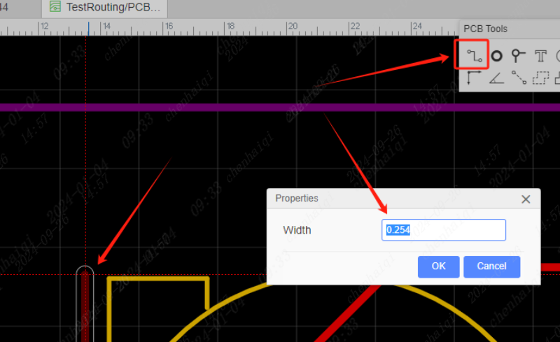
If you want to change the width of the wire from the beginning, you can change the rules for the wire width inside the design rules. 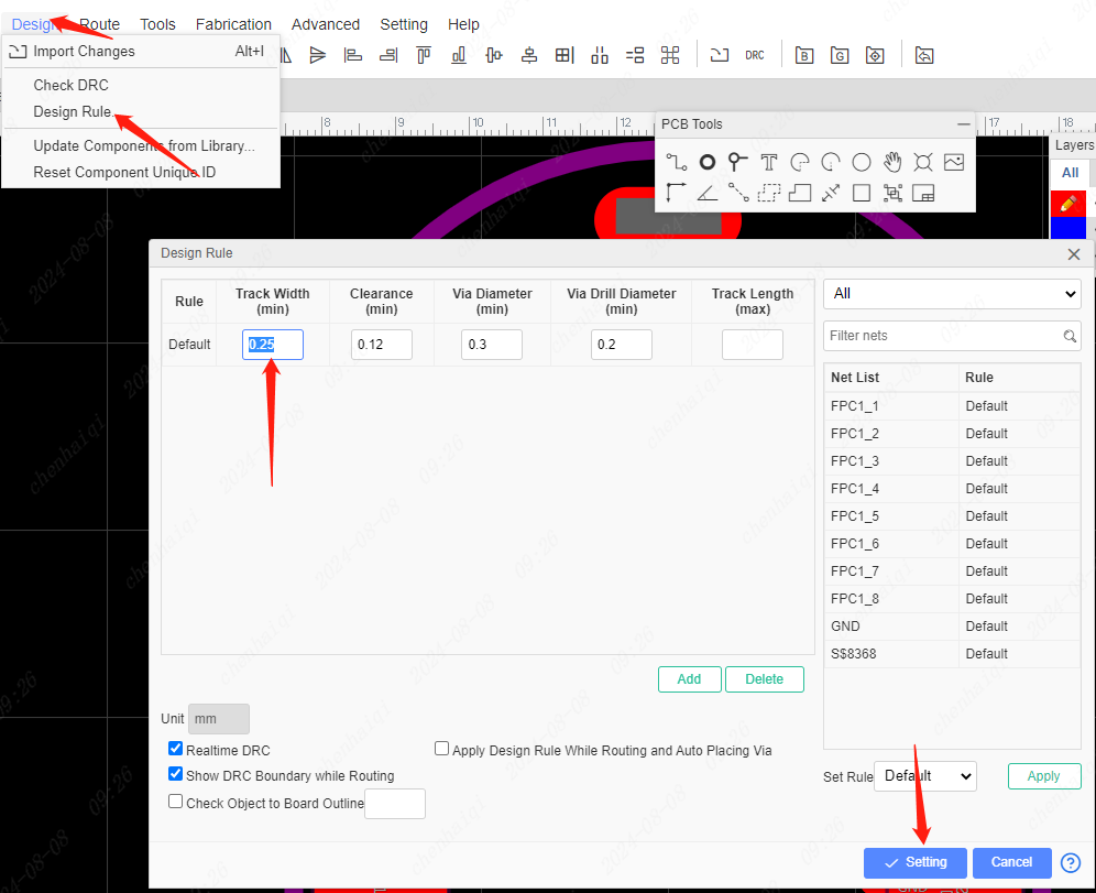
If you need to change all the wire widths in bulk, you can do this: The first step is to check "Track" separately for filtering. 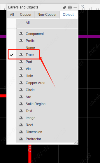
Then box the entire pcb and the system screens out all the wires individually.Finally, change the line width in the properties bar on the right.In this way, all the wires will change the wire width at once. 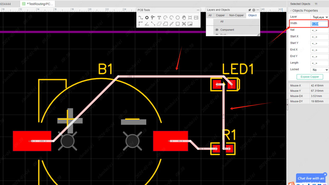
How to add or remove Suture vias?
Details
How to add: You need to select the copper, and then you can add it in the properties bar on the right. It is also possible to customize the size and distance of vias. 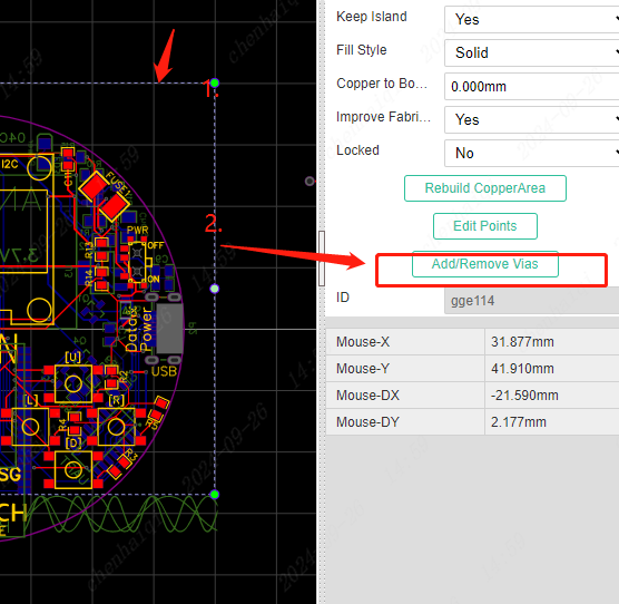
How to remove: Also need to select the copper, and then in the right property bar can be removed. It should be noted that the correct size and distance of the vias must be filled in when deleting, otherwise it cannot be deleted.
How to solve DRC spacing errors?
Details
Elements that are too close to each other will get an error if they exceed the design rules. 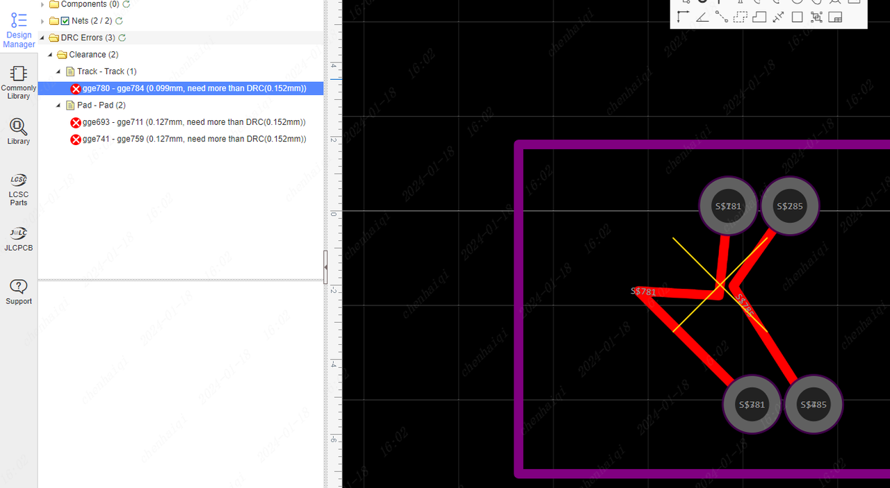
You need to change the space between the values in the design rules to be smaller, or make the space between the two elements larger in the diagram. 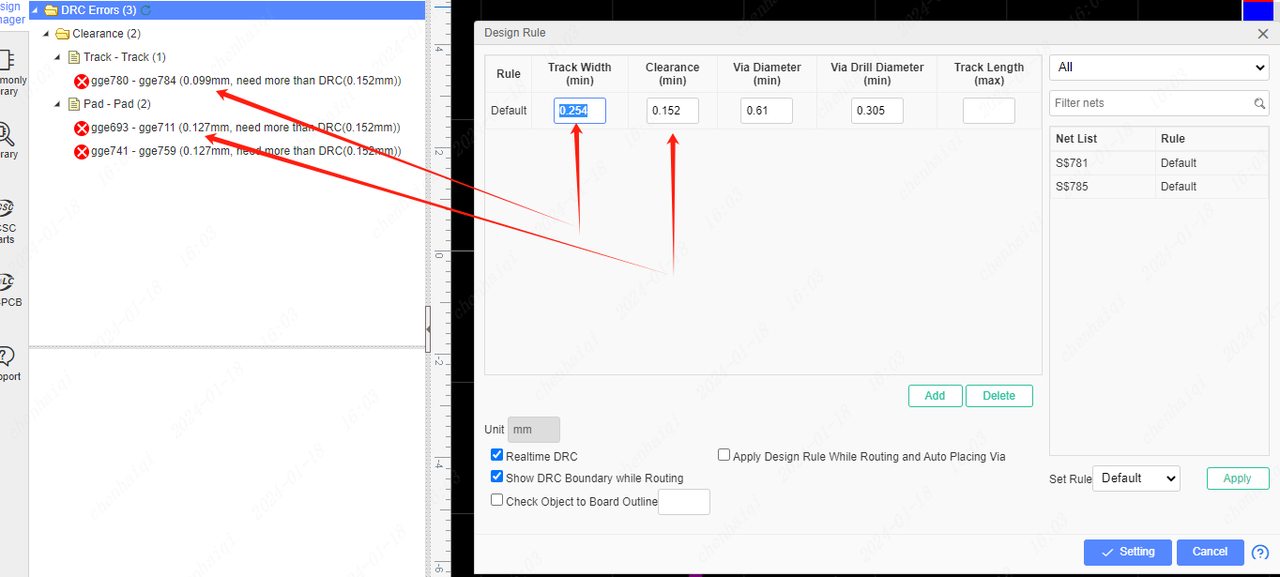
One thing to note: If it's the spacing between the footprints of the system libraries that is reported as an error, this is an error that can be ignored. This is because the footprints need to be drawn this way due to the needs of the physical device.
How to change the opacity of a layer?
Details
The layer manager can be accessed from the floating toolbar or the top menu bar.Then you can change transparency。 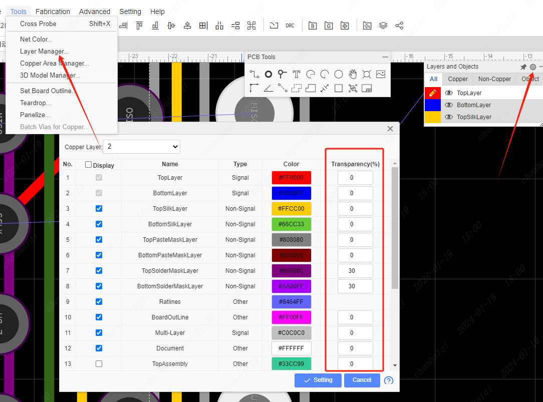
What if the copper area is not displayed after placing the copper area?
Details
First: do you place other elements of the same network in the copper area, if not then the copper area will not appear. Second: Check whether board outline is completely closed. 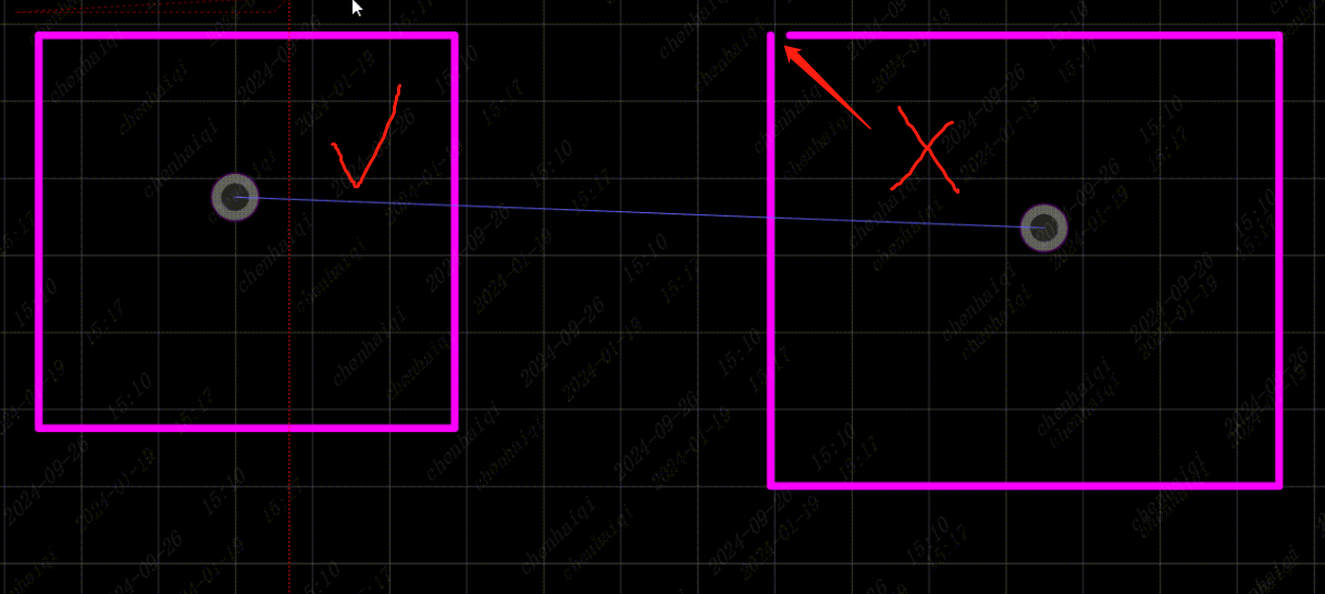
Third: There is no element corresponding to the same network in the scope of the copper area, but you still want to keep the copper area. You can click the copper wire frame, modify the property "Keep Island" in the right property panel and set it to "yes". 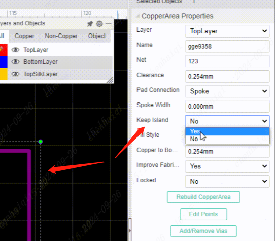
Fourth: When the same layer has more than one copper area at the same time, you can move the copper that is not shown up to the large copper through the copper manager. 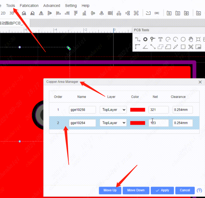
How to replace components without rewiring them?
Details
You can remove the unneeded components from the schematic and then replace them with new ones. Then click on the "Reset Component Unique ID" function at the top of both the schematic and the pcb.(Note: Click on both schematic diagram and pcb) 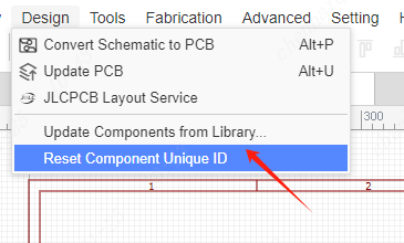
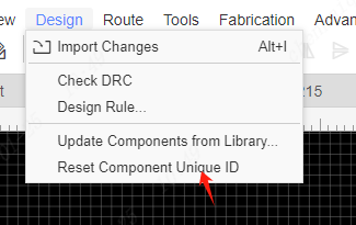
Second, go back to the schematic and click Update pcb. 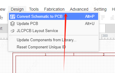
Finally, no global rewiring is required, only the wiring of the replaced component needs to be reconnected.
How would you change the sizes of all prefixes in bulk?
Details
First, select prefix separately in Object. 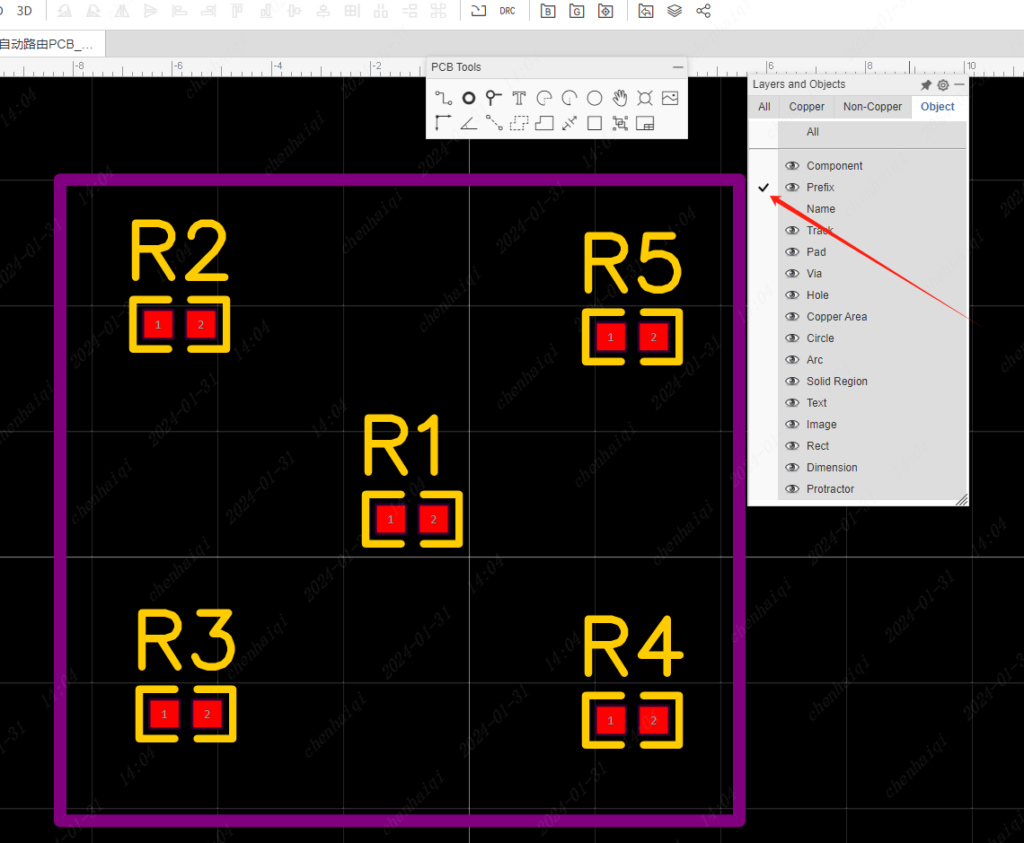
Next, select the entire selected area, and the prefix will be filtered. Finally, go to the right property bar and change things like font size or Angle. 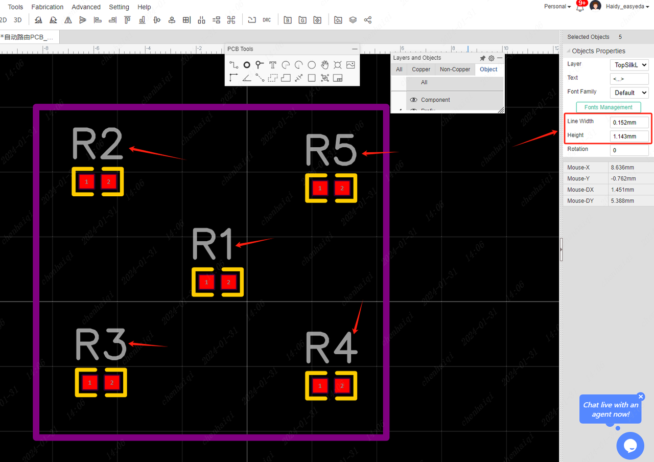
How to make a ring pad?
Details
Using the two-point arc wiring method, draw two semicircles and then turn them into pads individually. 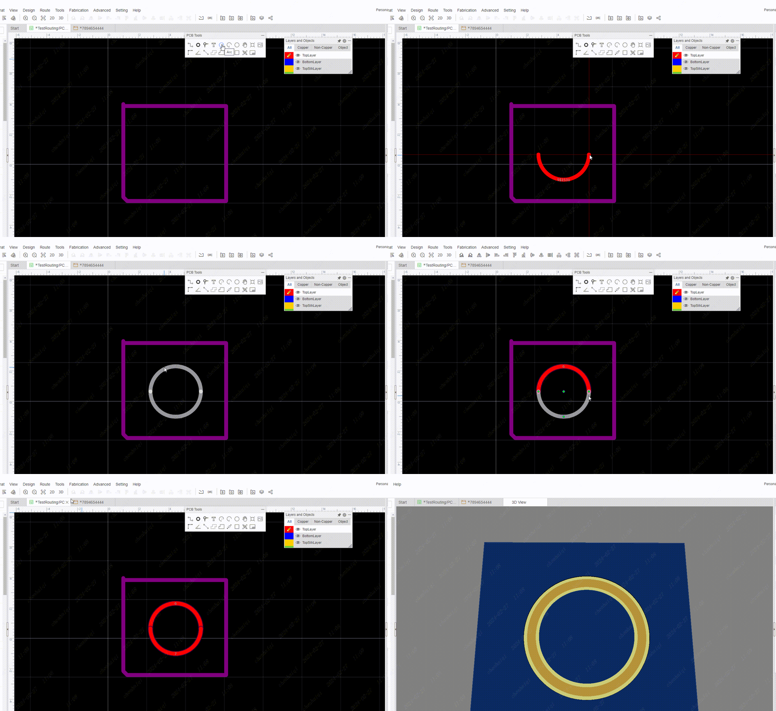
How to set the position of component Designator or Name in bulk?
Details
Firstly, you need to box the board in its entirety.Next, select the “prefix position” Tools in the top menu bar. 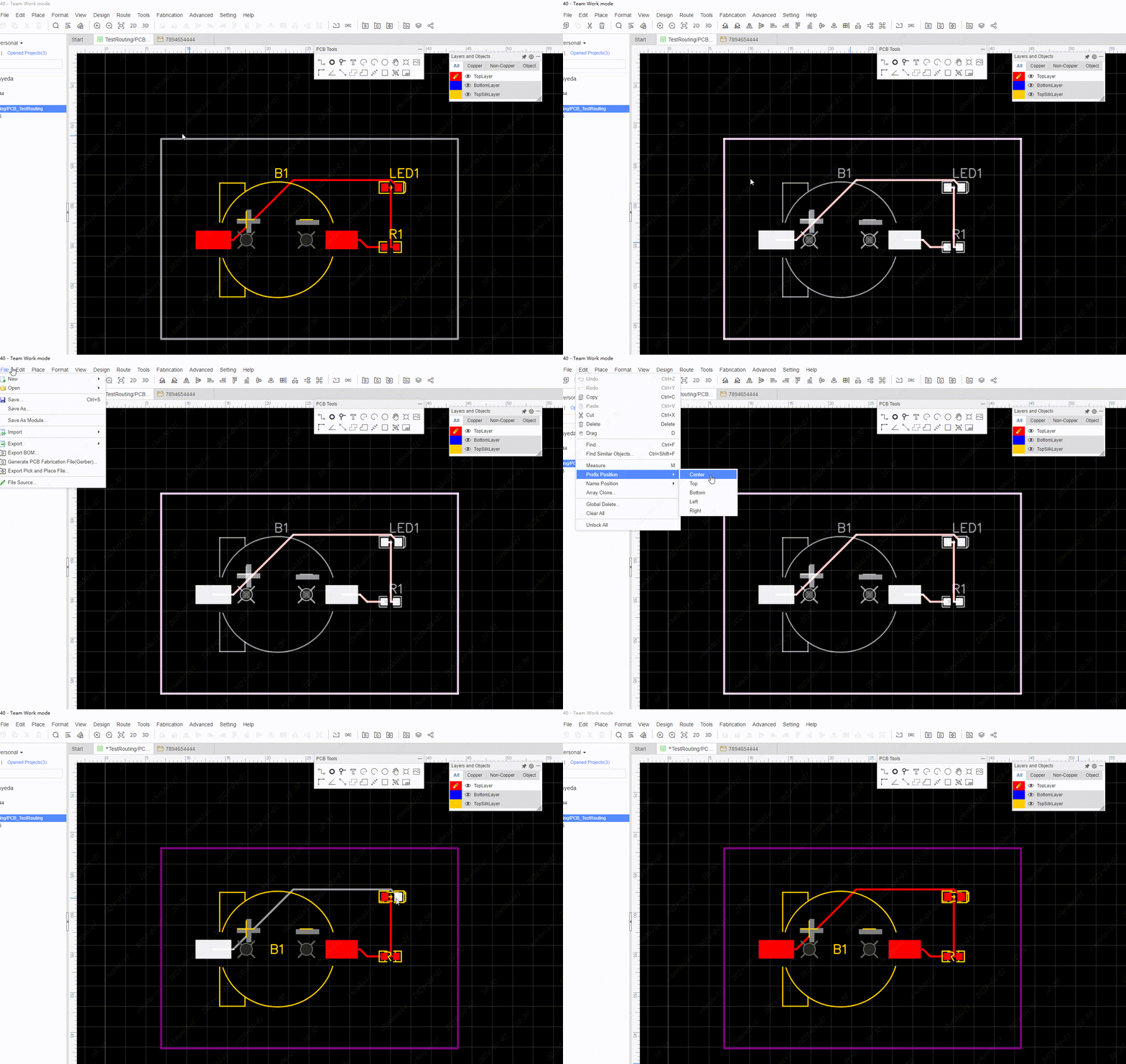
How to modify the “plated”of the pad?
Details
Select the pads to select them in the Properties column on the right. 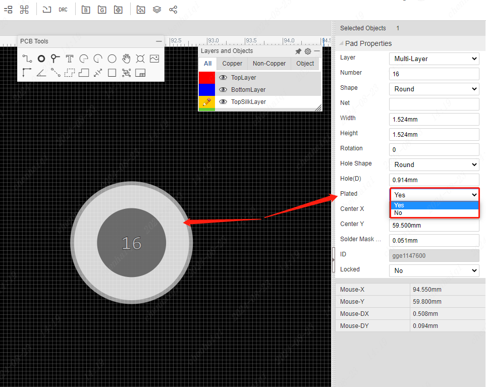
It should be noted that once the ‘plated’ setting of the pad is set to ‘no’, the pad loses its electrical properties and the inner wall of the through-hole is copper-free. It is often referred to as "Nine plated though hole (NPTH)".
How to change the color of a layer?
Details
Go to the layer manager from inside the settings in the top right corner and we can see the colors of each layer.Note that the colours modified in the Layer Manager are for all elements of this layer. 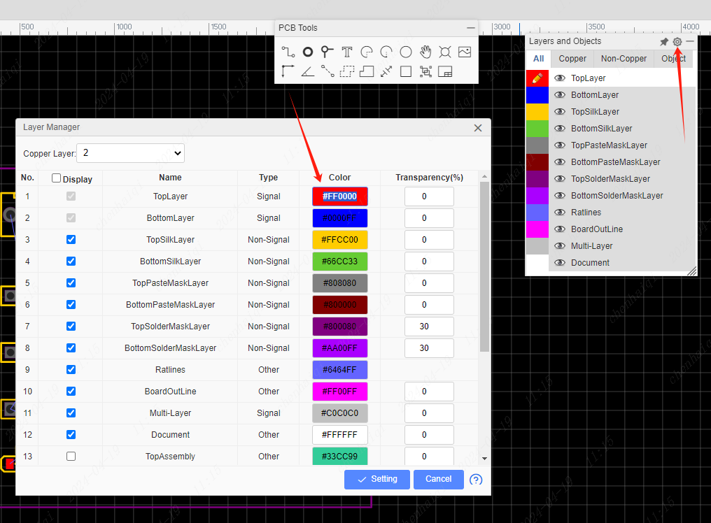
Currently, there is no way to modify the colour of an element individually in the Standard Edition, so if there are designers who need this feature, they can use the Professional Edition. 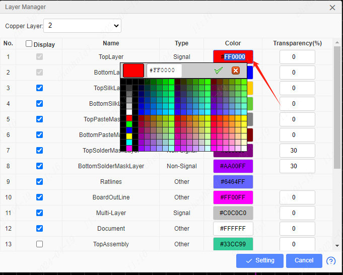
How to flip the footprint?
Details
Inside, the standard version does not support one-sided mirrored packages, only the footprint can be switched top or bottom. If you want to place components on the back of the board, you can switch layers. The top layer is the front side and the bottom layer is the back side. Components placed on the bottom layer will have a mirrored effect, which is only a normal view phenomenon. 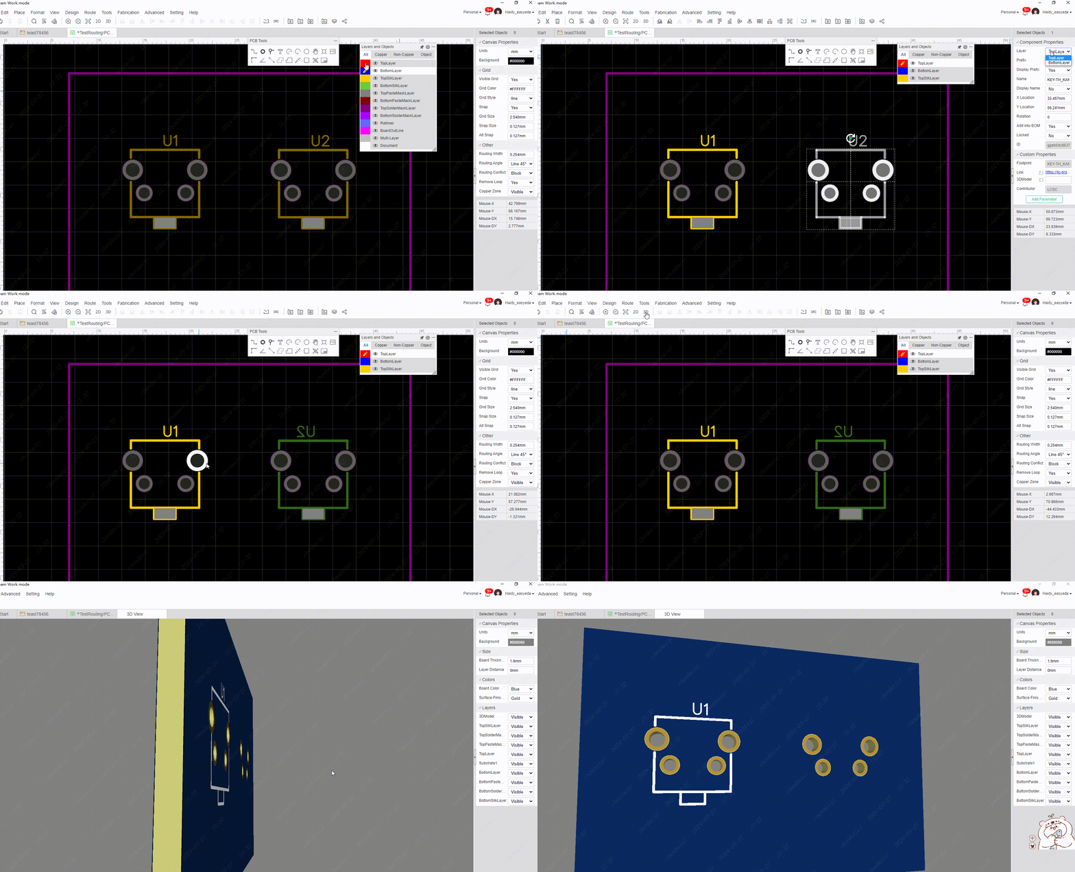
How to bind and change footprint?
Details
When we find that a component has no footprint, we can click on the component and click on the footprint manager in the properties bar on the right. 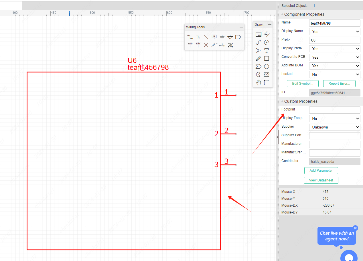
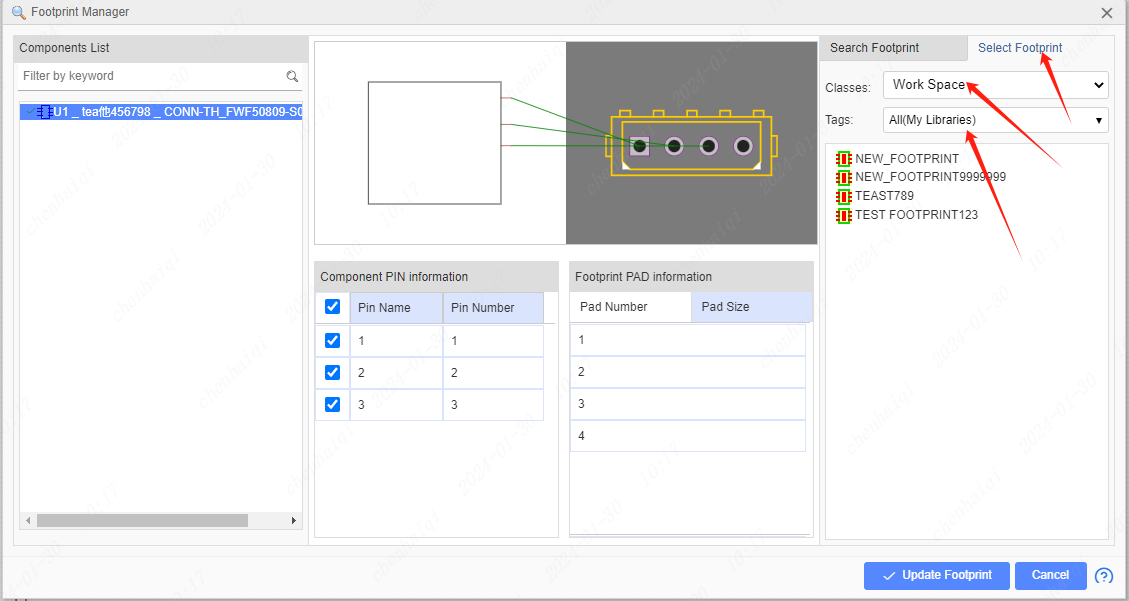
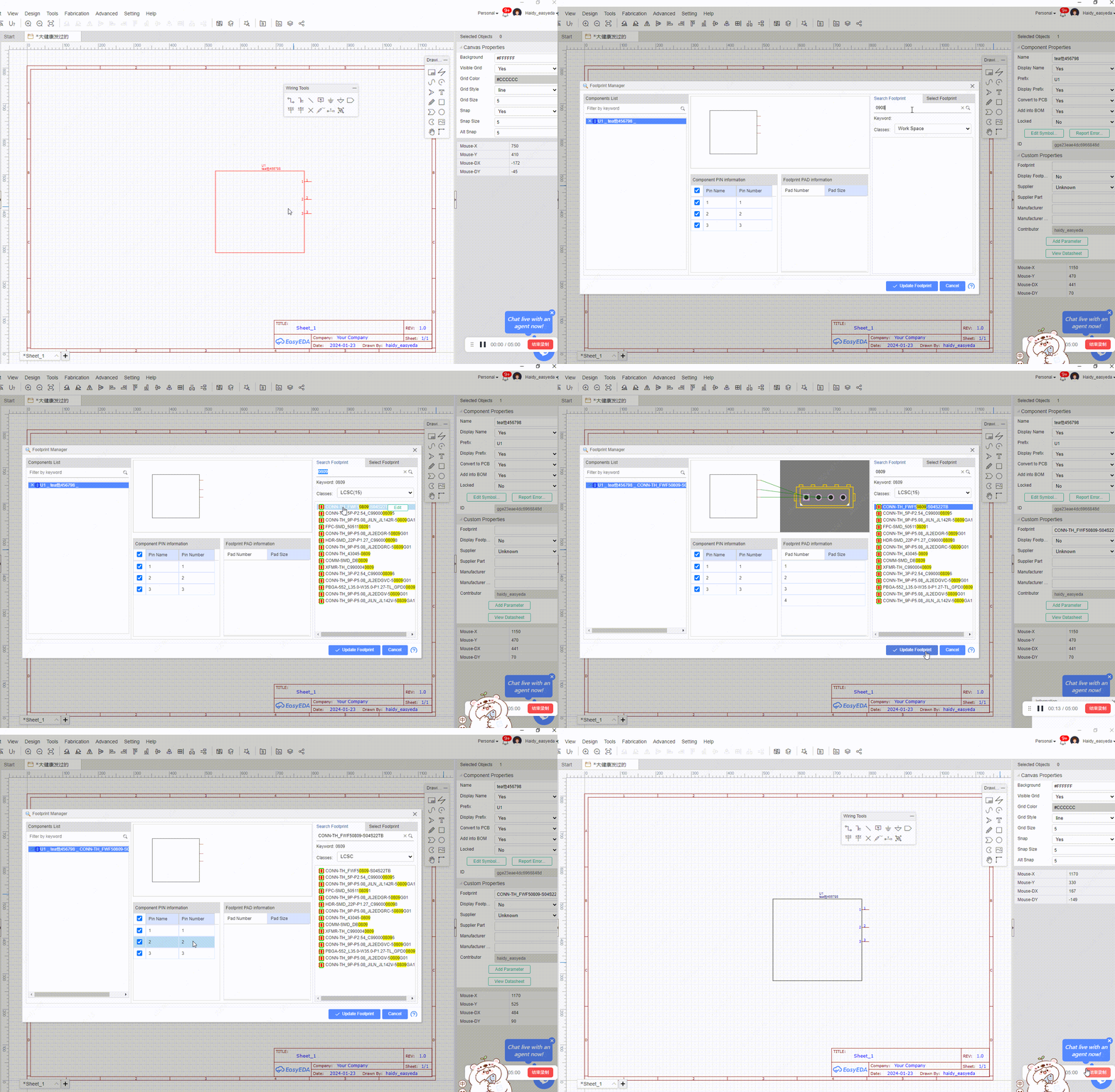 In the footprint manager, you can help components bind the footprint of the system and replace the footprint. In addition, if the system library does not have the footprint you want, you can choose to draw your own footprint to bind.
How to Expose Copper to Wire?
Details
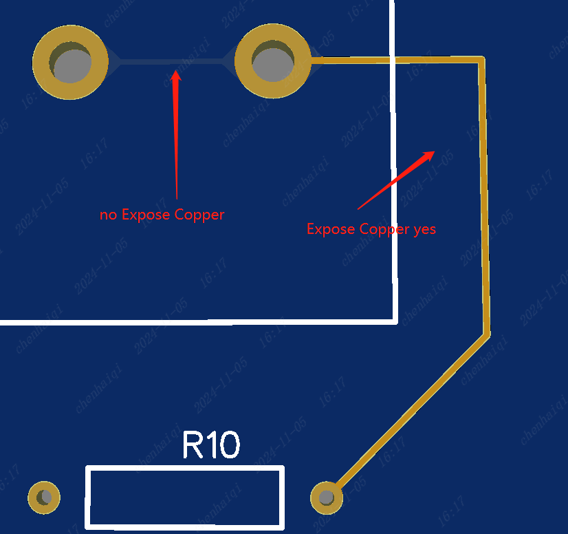
Click on the wire, click on ‘Expose Copper’ in the right property bar, and finally you can see the effect in the 3d preview. 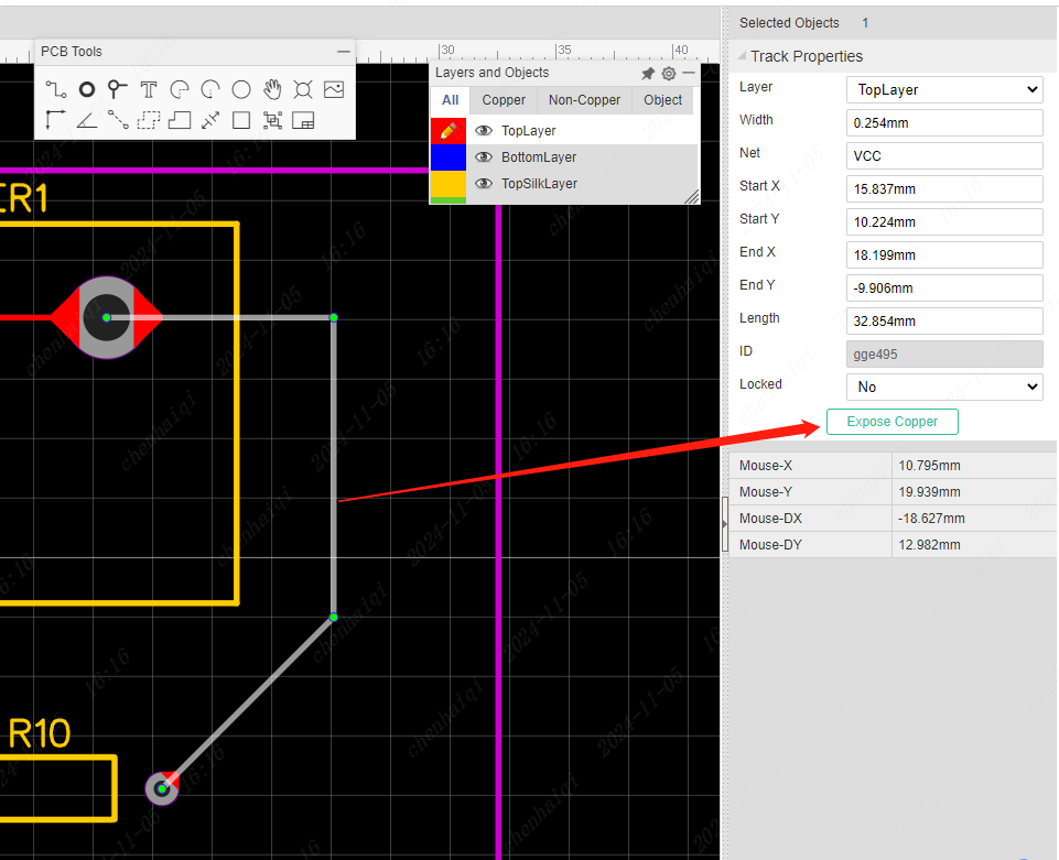
How to draw the Slot Region?
Details
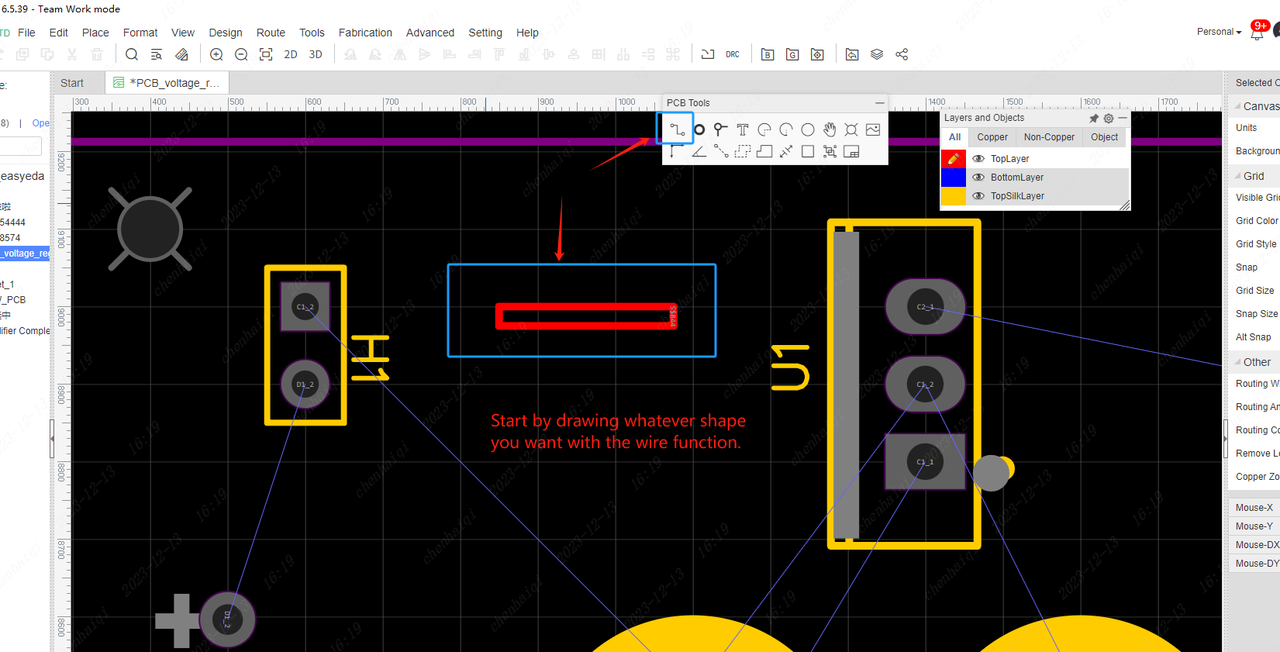
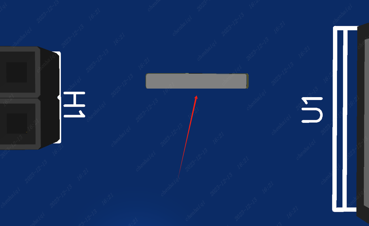
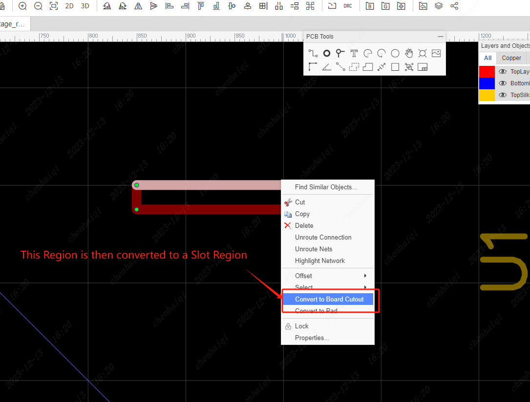 It will become this effect displayed in 3d preview.
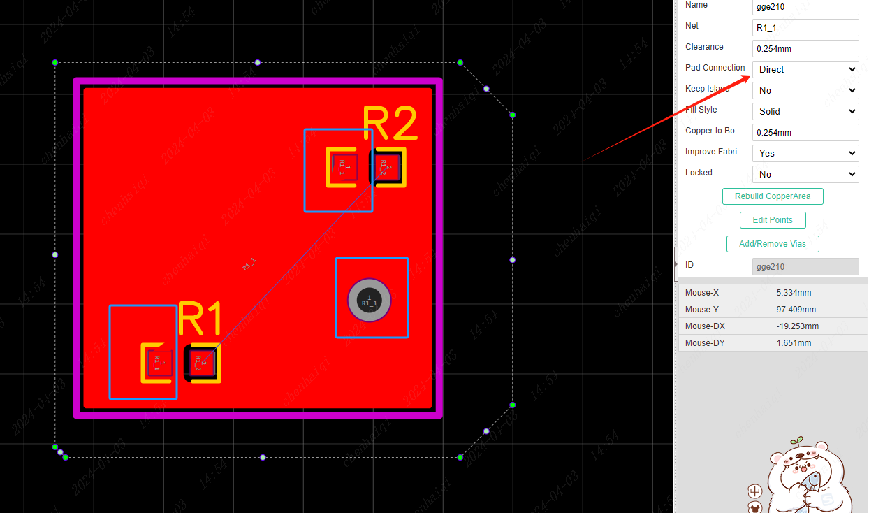
How to modify the connection between the copper area and the pads?
Details
First select the copper-laying area, and then you can modify the connection method in the property column on the right. 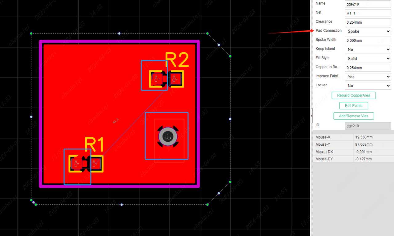
How to expose the copper skin in the copper laying?
Details
It is only necessary to overlay a layer of solder mask on the copper to leak out the copper. 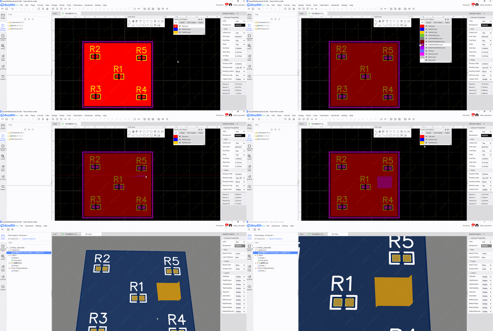
How to set up automatic teardrops for wires?
Details
Find ‘System Settings’ in the settings on the top menu bar and then tick the option to add teardrops automatically in the pcb. 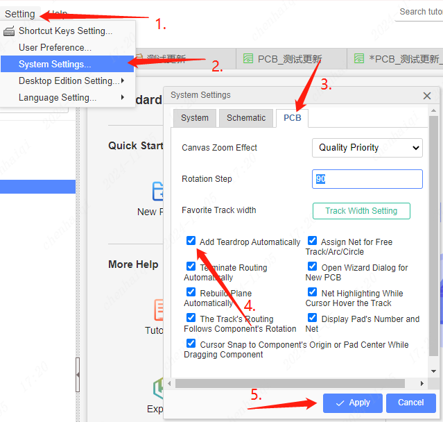
How to highlight and unhighlight networks in PCB?
Details
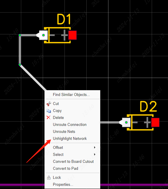
Just select the web element and click the right mouse button. 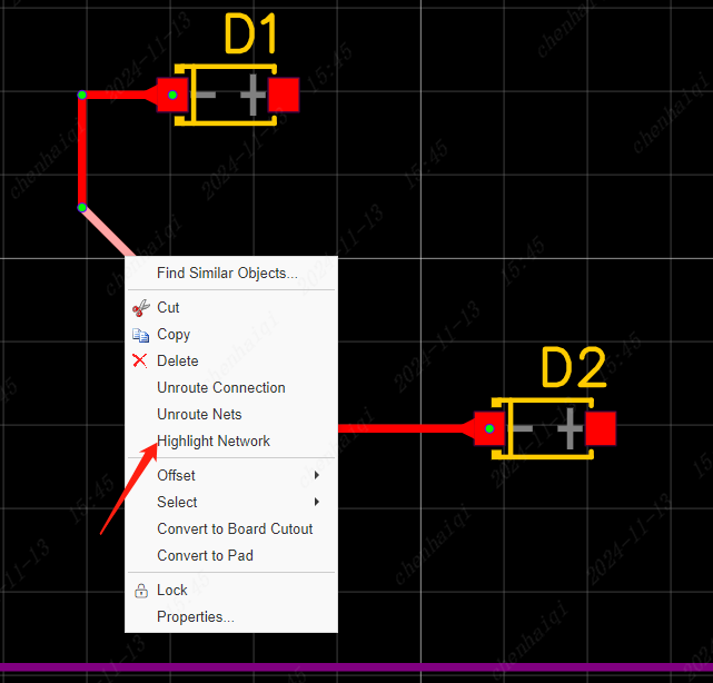
How to set the text to remove the green oil leaking out of the copper skin?
Details
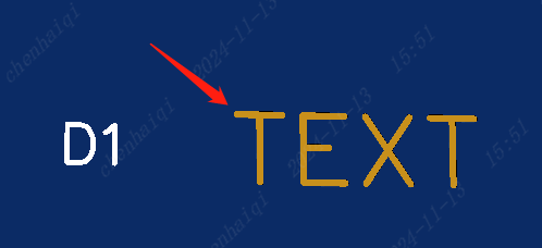
Place two texts at the same time in the top layer and the top soldermask layer and then overlap them. Then you can see the effect in 3d preview, the yellow text indicates the leakage of copper skin. 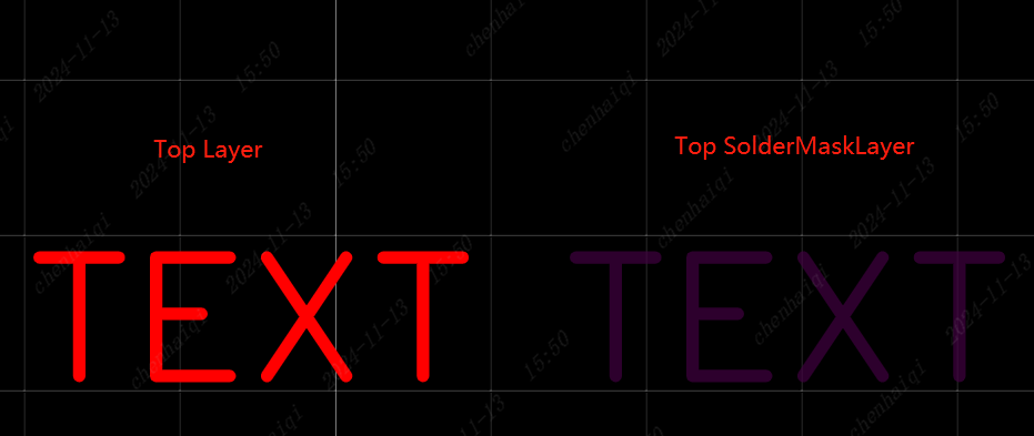
How to batch delete wires on the same network?
Details
Find Network Tools on the left, select the network you want to delete, click on it and after you see all the network wires highlighted, move your mouse over the canvas and click the right mouse button to delete it. 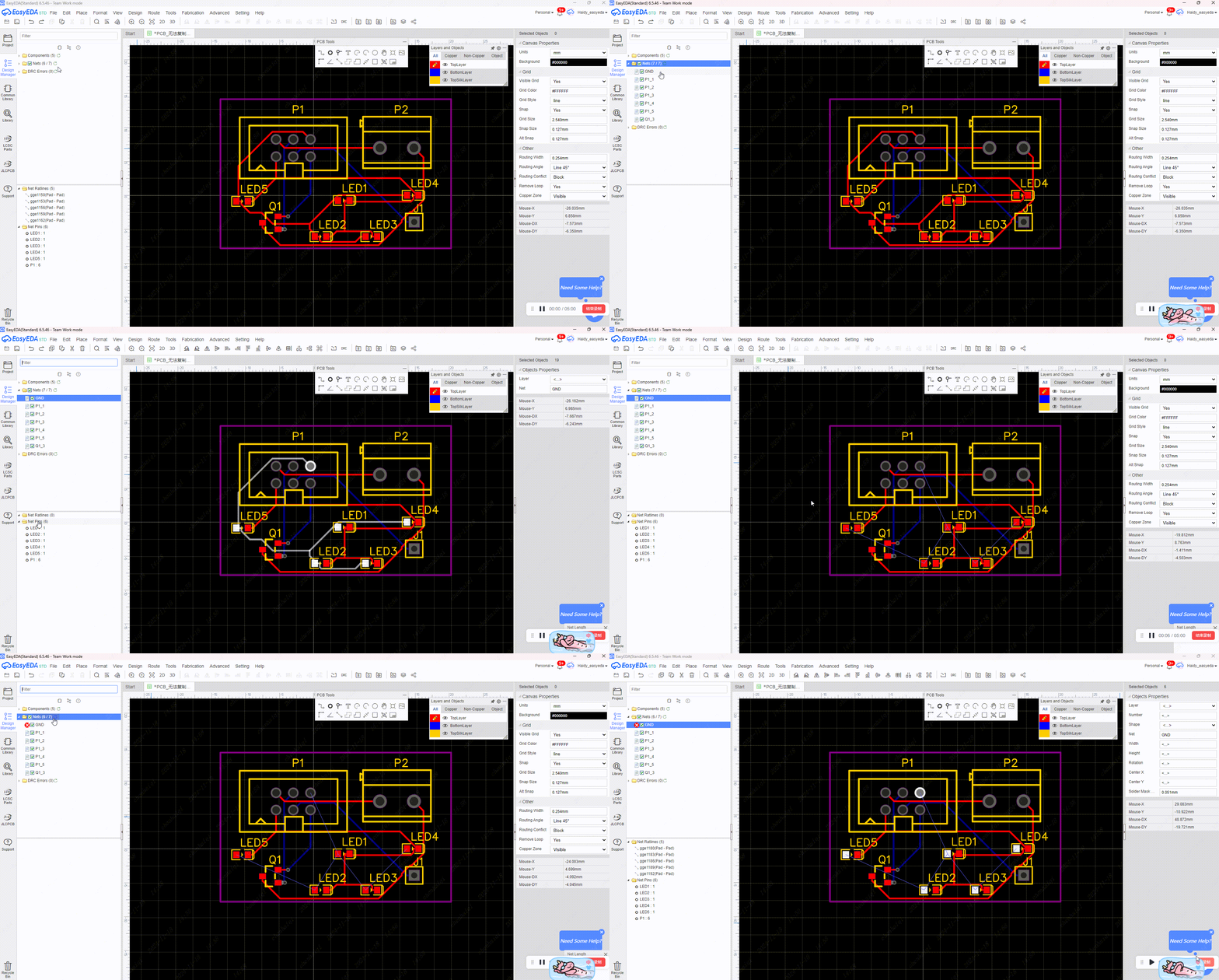
How do I batch change the size of the via?
Details
We can use the ‘object’ toolbar to individually select perforations or other elements, and then sift through all the selected objects after selecting the area, and finally make batch modifications in the right property bar. 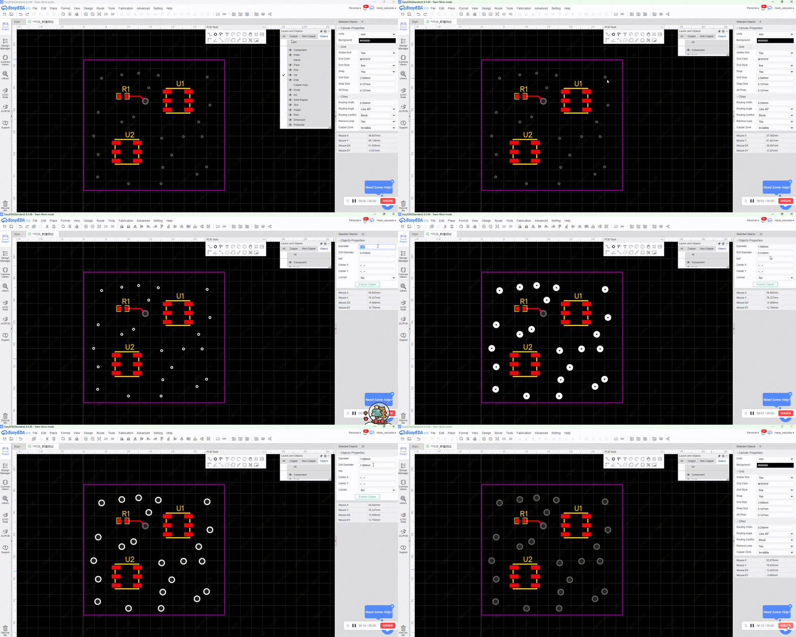
How do I set up different network rules?
Details
Find the ‘Design Rule’ menu in the top menu bar. Once you are there, you can add the design rule you want and then select a different network to use the new rule on the right. Then you can select different networks to use the new rule. It is important to note that the design rules are network based, they can only be categorised by network. 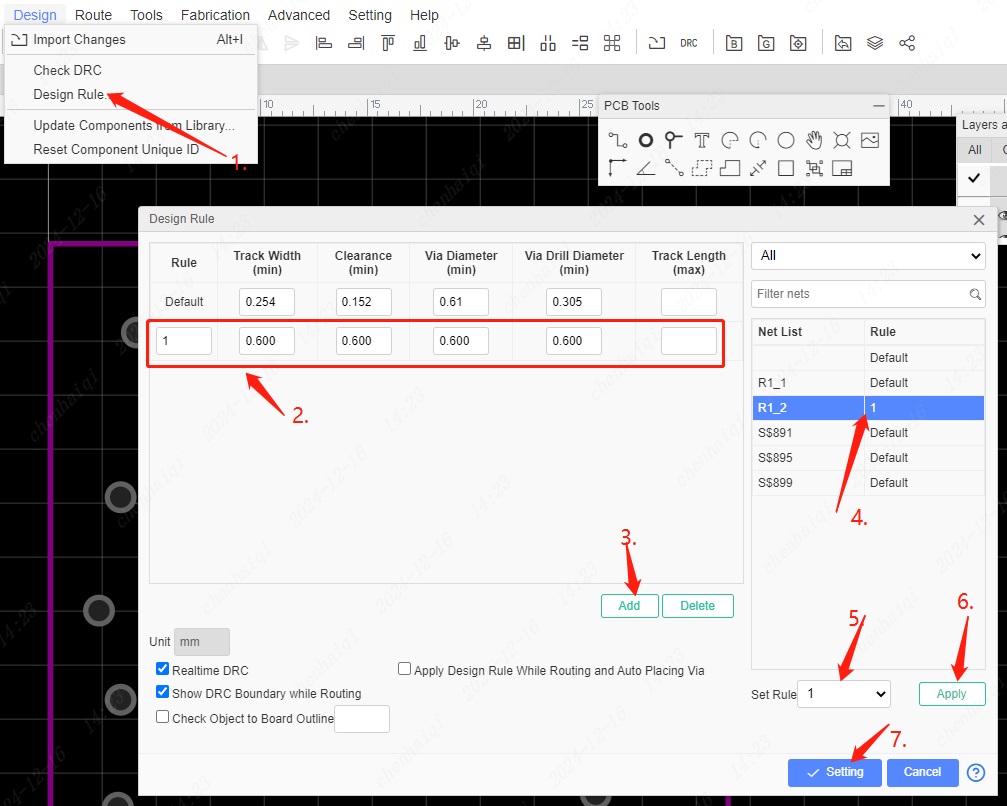
How to place new board outline?
Details
This can be done when we need to relocate or draw a new board outline in the PCB: You can find the ‘set board outline’ function in the tools section of the top menu bar, and then select the shape and size of the board and the line width according to your needs. 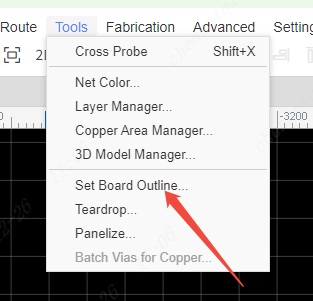
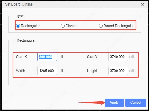
You can also choose to set the layer brush on the board outline layer and draw the desired polygonal board frame yourself. 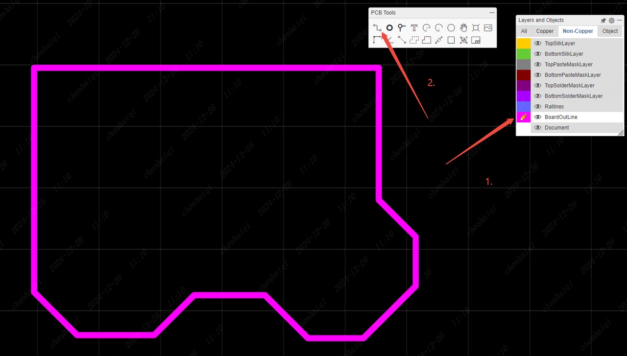
How to set the wires to follow the footprint movement?
Details
If you want the wires to move with the footprint when you move the footprint in the pcb, then you have to tick this feature in the settings. 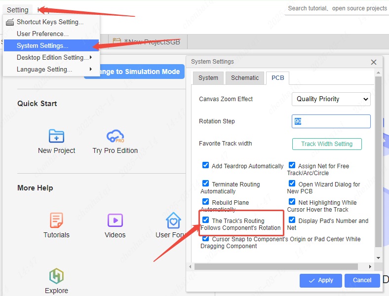
How to quickly modify the spacing between paving copper and elements?
Details
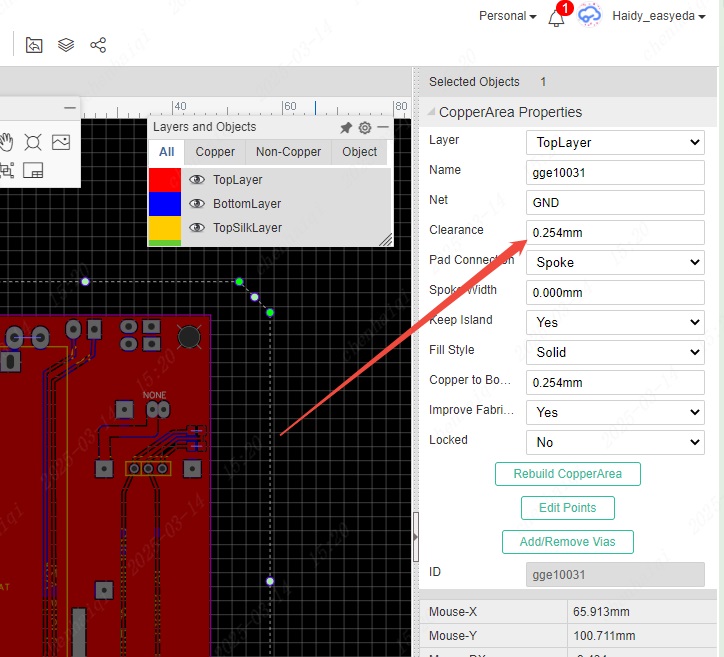
When we need to modify the spacing between the copper-laying area and the element after copper-laying, we can do so:
- Select the copper-paved area.
- Click the right property bar to modify the Clearance. Note: In general, after setting the spacing, the copper paving area will be updated automatically, if the system does not update automatically, you can use the shortcut key ‘shift + b’ to rebuild the copper paving, this step can prevent the subsequent board errors.
How do pads and vias leak copper?
Details
Under the default settings, the pads leak copper and the vias do not leak copper. Like this:  If you want the pad to be copper-proof, change the value to -500mil in the property bar on the right.
 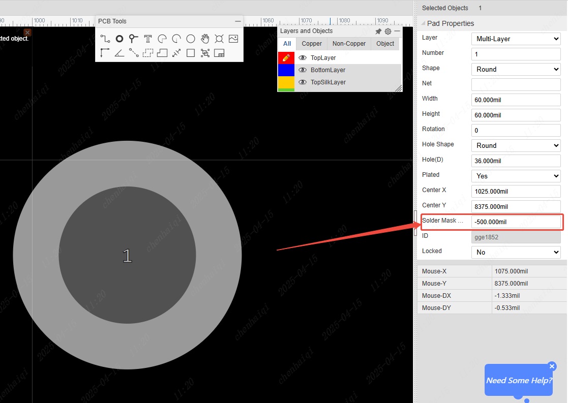 If you want the via to be copper-exposed, click "expose copper" in the property bar on the right.
 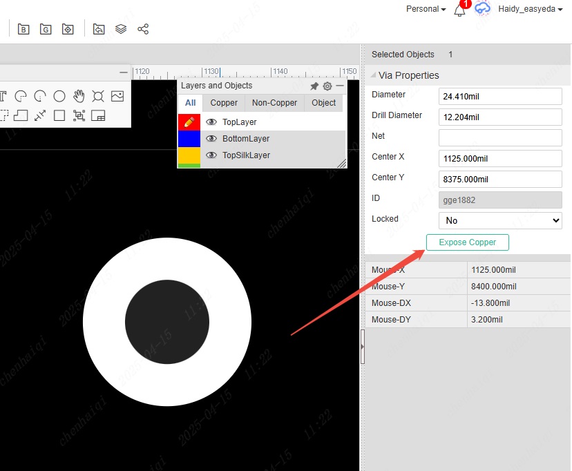 Like this:
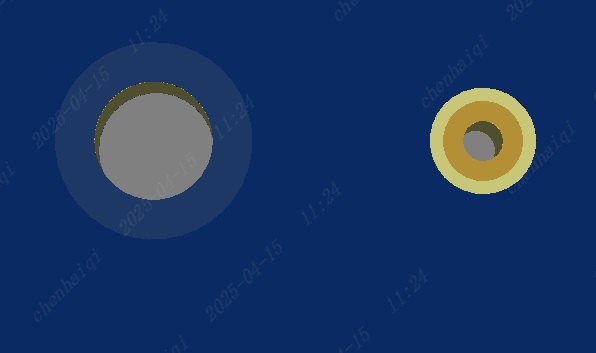
How to enable or disable the snap feature?
Details
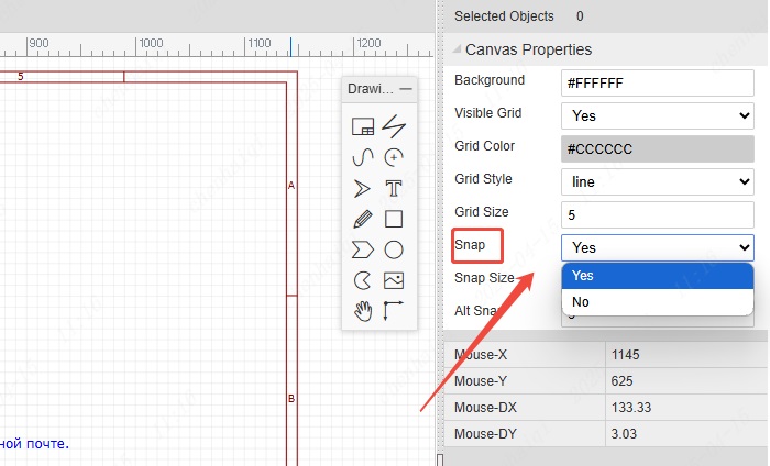
The snap function can be found in the property bar on the right side of the PCB or schematic. 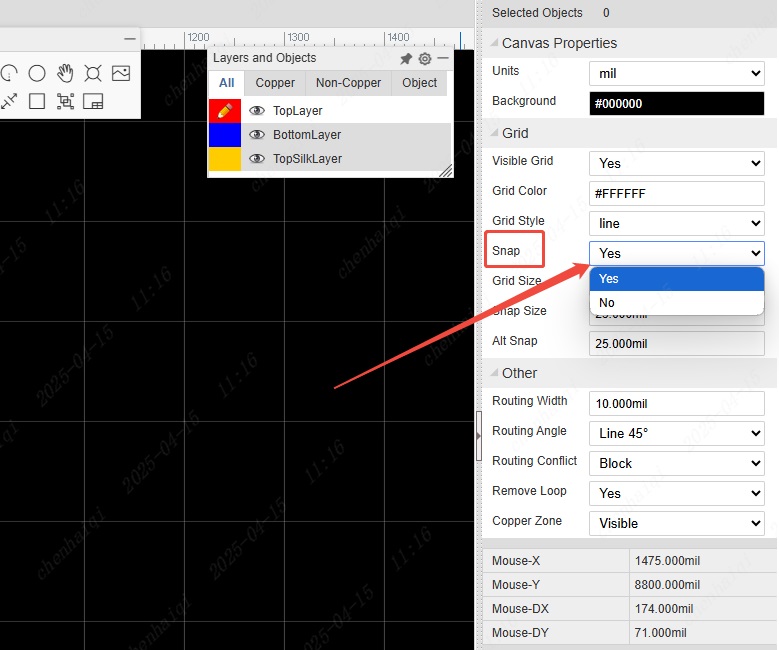
How to choose to display or not display the network name and pad number in PCB?
Details
In the settings on the top menu bar. 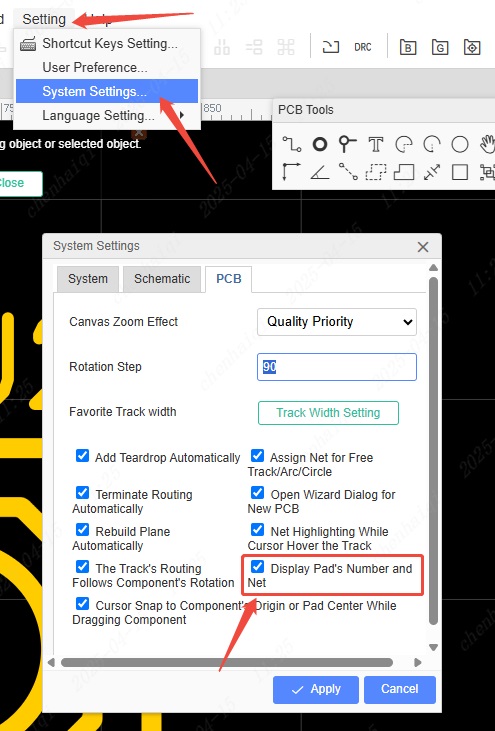
How to check footprint size?
Details
If you want to see the exact size of the footprint, double-click on the footprint window in the Library tool. 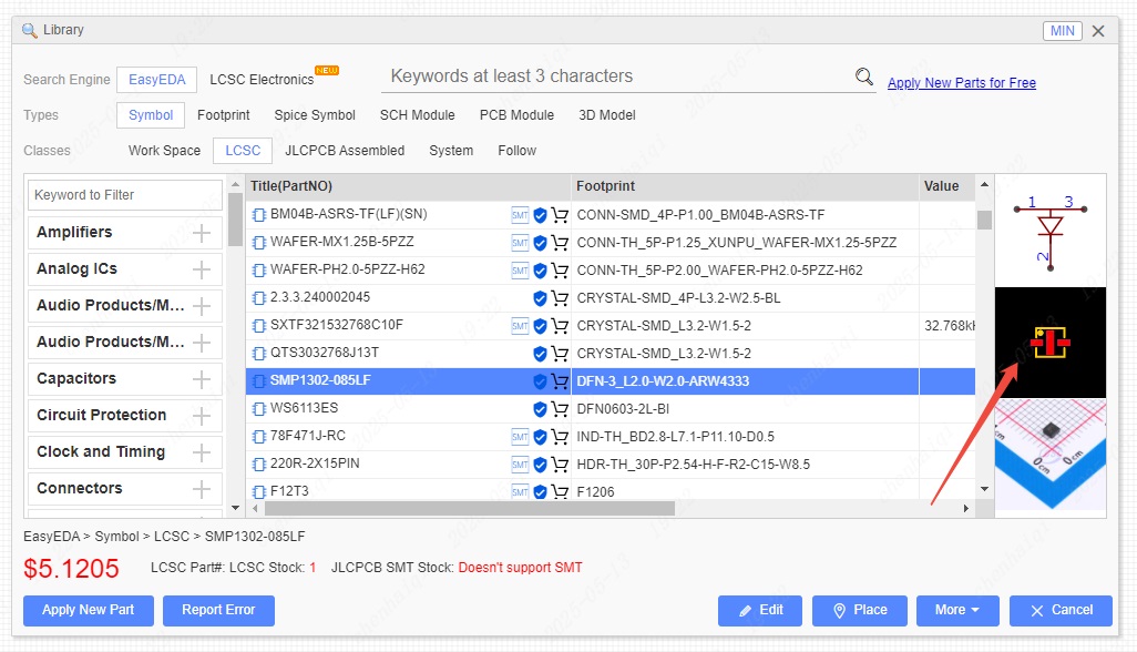
After entering the footprint interface, you can use the smart size tool to view it. 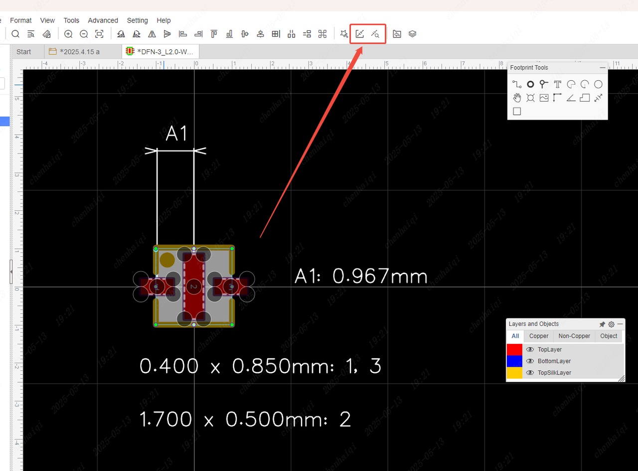
If you want to know the pad size of the footprint more quickly, you can check it in the footprint manager. 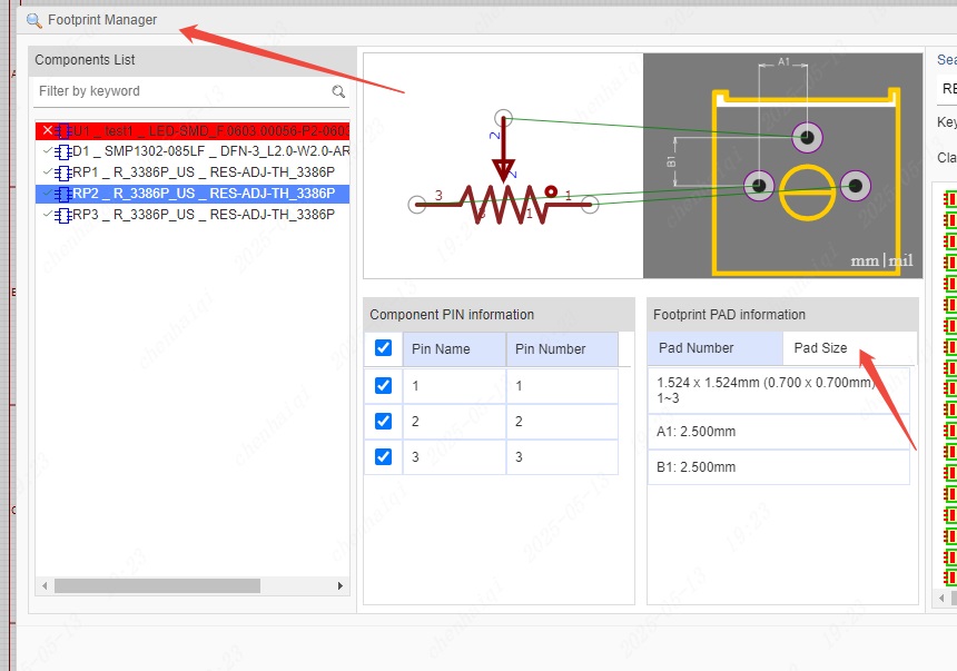
How to set the spacing between different networks and copper plating?
Details
We can achieve different spacing effects between different network elements and copper plating through network-network design rules. For example: My design has two networks, VCC and VDD. I want to place a GND copper area with a different spacing from the two networks. 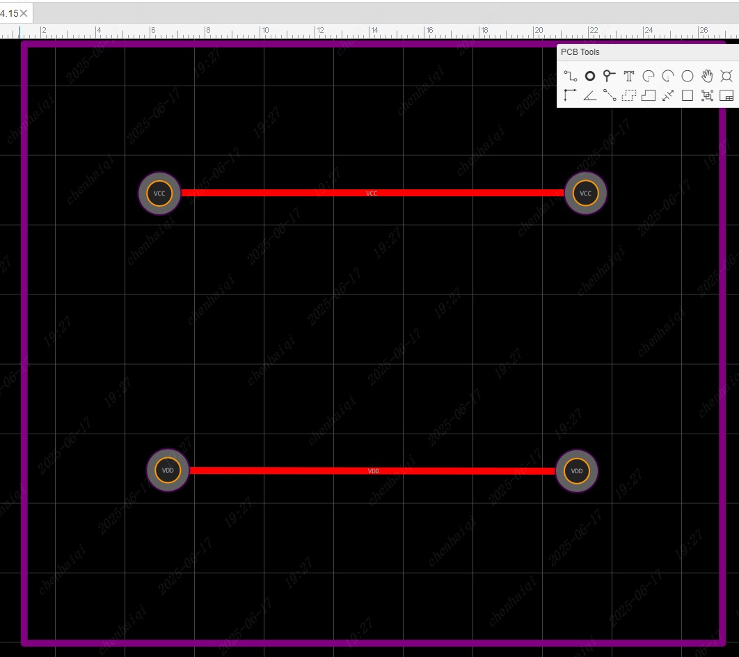
First open the Design Rules panel, then create the two spacing rules you need and apply them in the Rule column on the right. 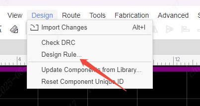
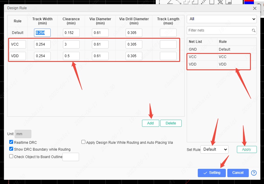
Finally, you can see two different spacings by plating copper. 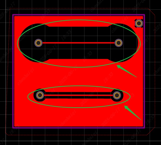
How to modify the wiring angle?
Details
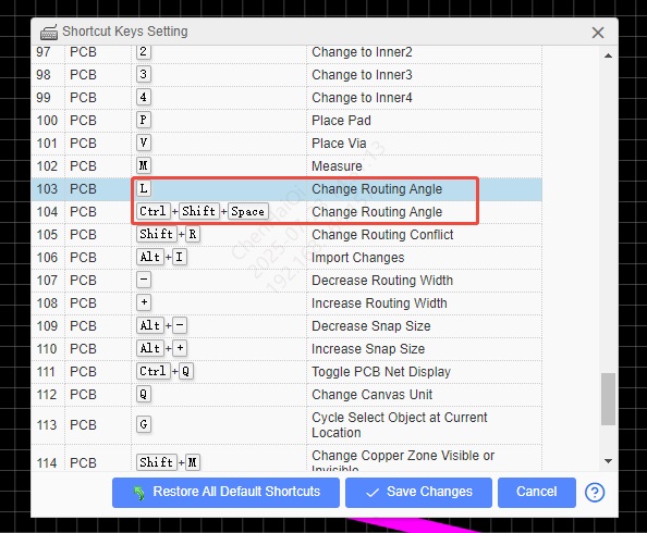
We have five different wiring angles for users to draw wires and lines. You can switch them to the right menu bar or use shortcut keys. 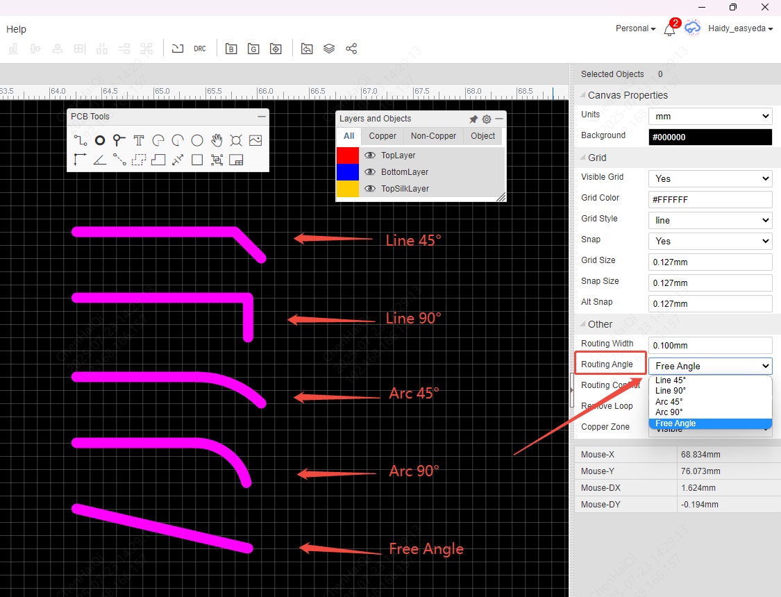
How to set line width in Auto Route?
Details
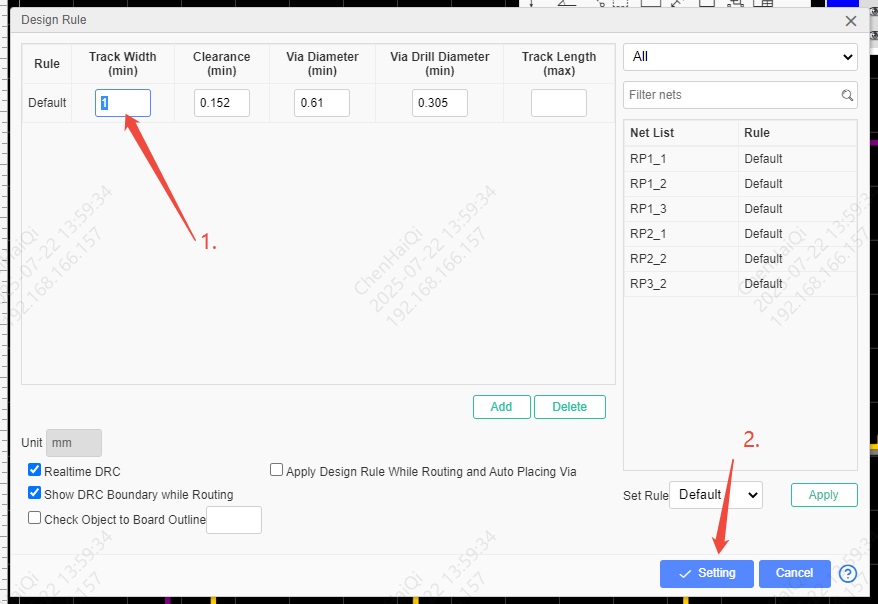
First, modify the value of the routing width in the design rules, click Confirm, and then perform Auto Route. In this way, the routing width of Auto Route can be routed according to the thickness you want. 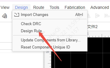
How to batch display/hide device properties in PCB?
Details
First, we check the "component" option in the "Objects" column in the "Layers and Objects" panel. 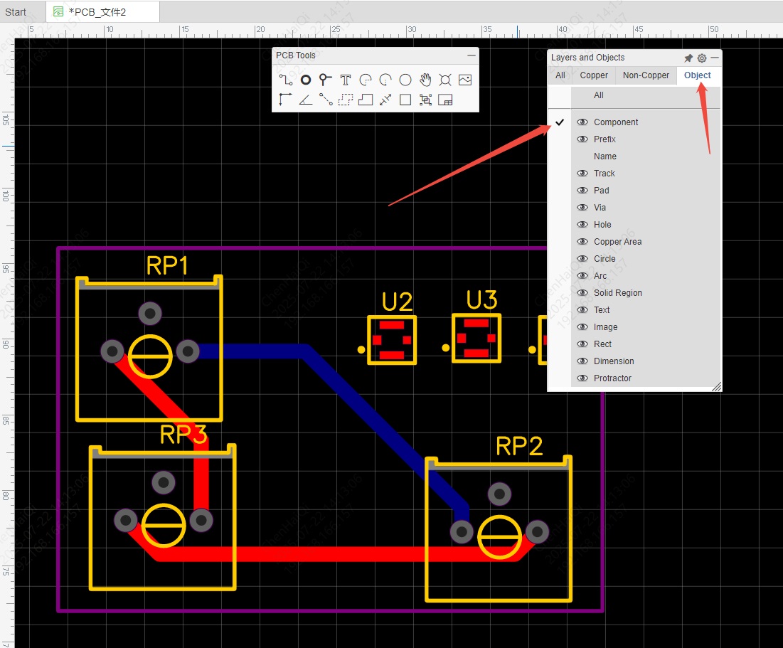
Then select the entire PCB, and the system will automatically filter out all device elements for you. Finally, you can hide and show Prefix and Name in the property bar on the right. 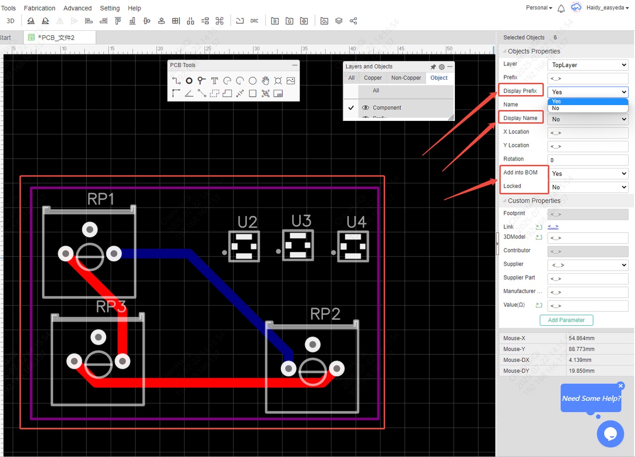
How to change layers using shortcut keys?
Details
When you want to quickly switch between the top and bottom layers during wiring, you can use the shortcut key "shift + */ *", which is the default shortcut key of the editor. (Of course, if you don't like this shortcut key, you can also modify it.) When you need to connect the top and bottom layers of the same wire when drawing, just use the shortcut key to switch layers. After the connection is completed, the system will automatically add vias to the nodes of the top and bottom layers for you, and you don't need to add them yourself. Any shortcut keys can be found and modified here. 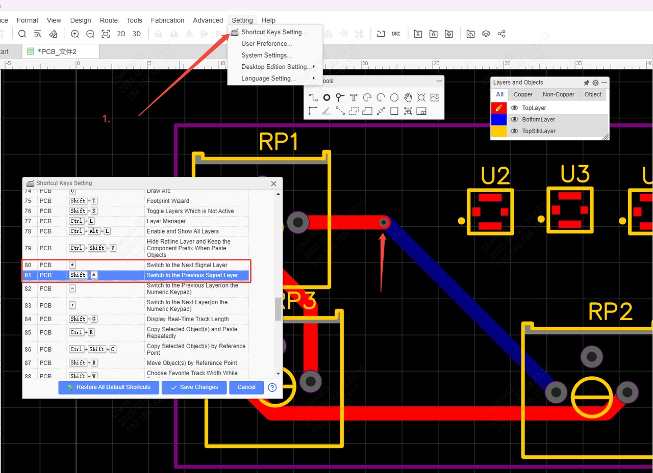
Why can't I select any element on the canvas?
Details
When we suddenly cannot select any element in the canvas, we can first check whether the "Objects" option in the "Layers and Objects" column is checked. You can also consider this reason when you suddenly cannot select one of the elements. If there is no check in the "Objects" column, it means that the element is not selected, and all the elements in the canvas cannot be selected. 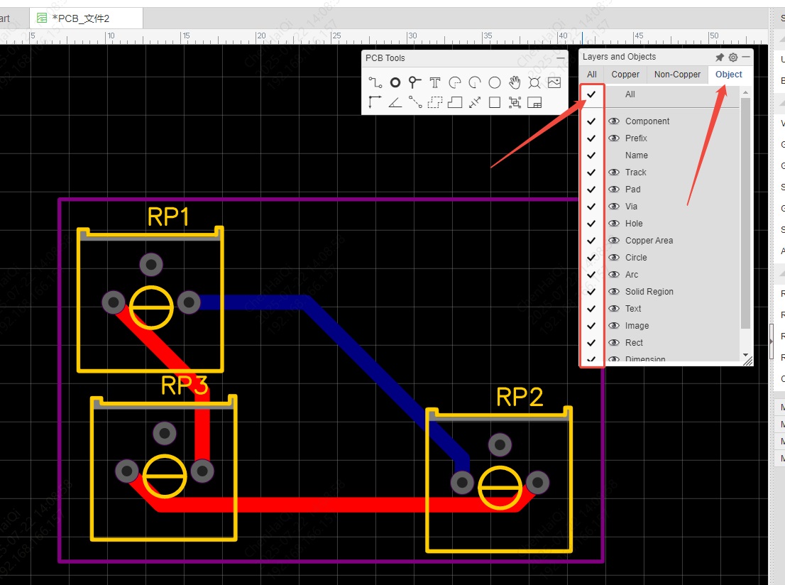
If checking the previous option doesn't work, you can also check if the element is locked. You can find the "Unlock All" tool in the top menu bar. 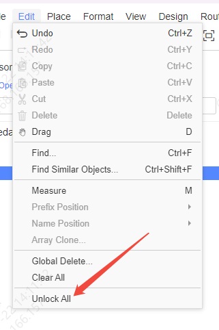
How to create rectangular pads?
Details
Click on the pad, and you can change its shape to a rectangle in the properties panel on the right. However, EDA does not support creating rectangular drill holes, so the drill hole shape cannot be changed to a rectangle. 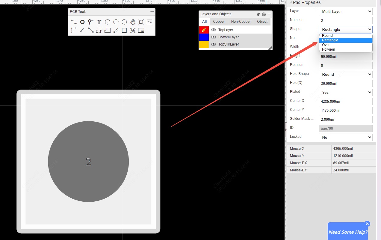
How to delete a device's 3D model?
Details
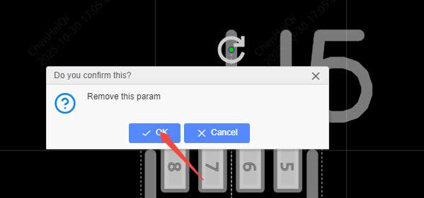
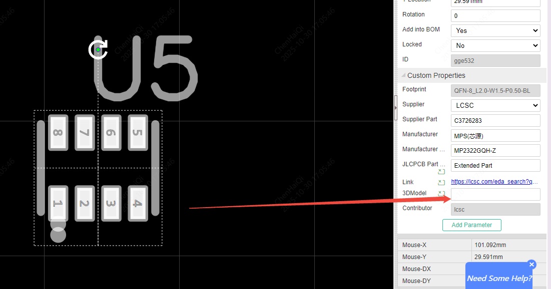
Click on the device, and you will find the 3D model input box at the bottom of the right-hand properties panel. Then click the delete button. 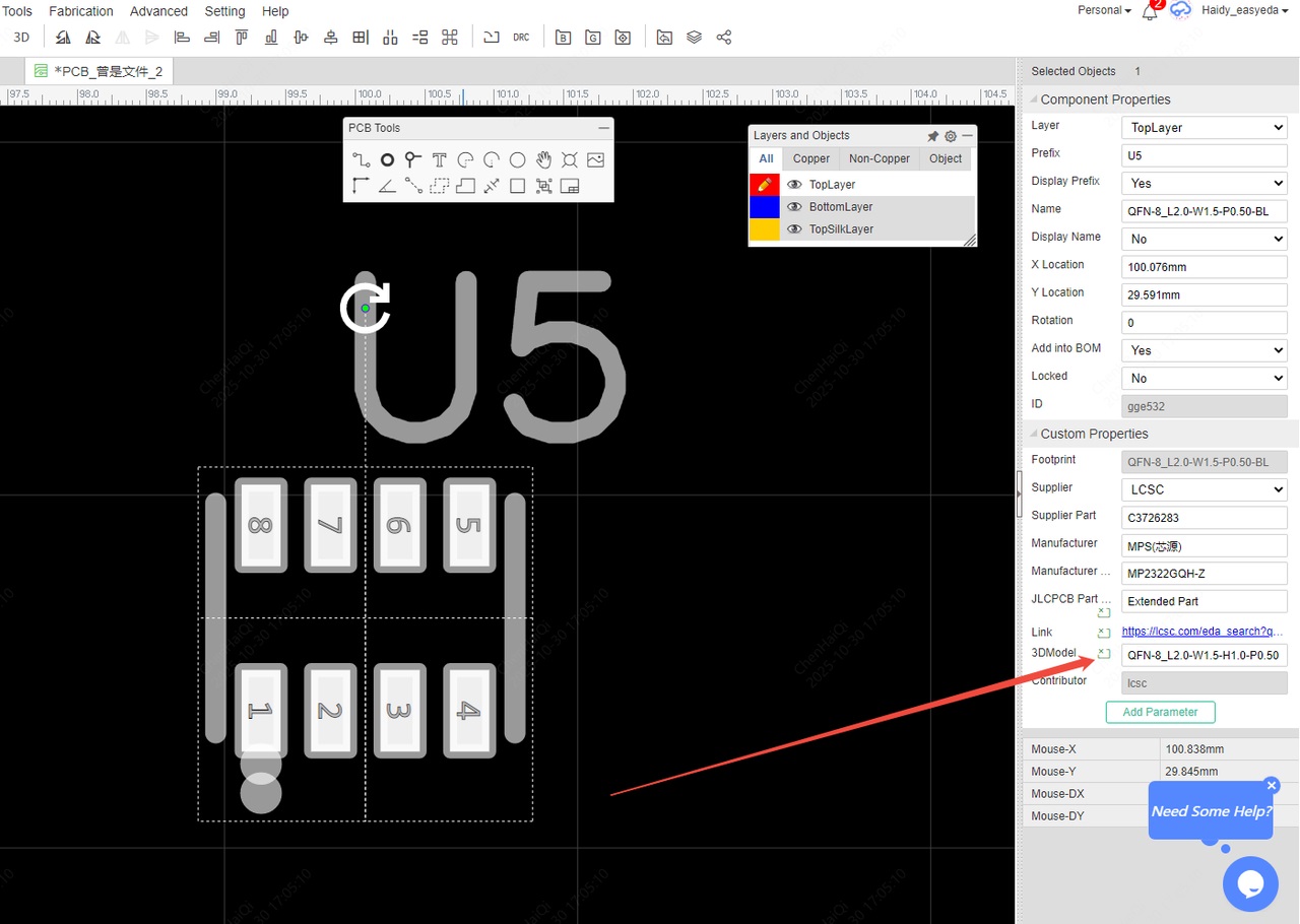
How to modify the divergence linewidth of copper pour?
Details
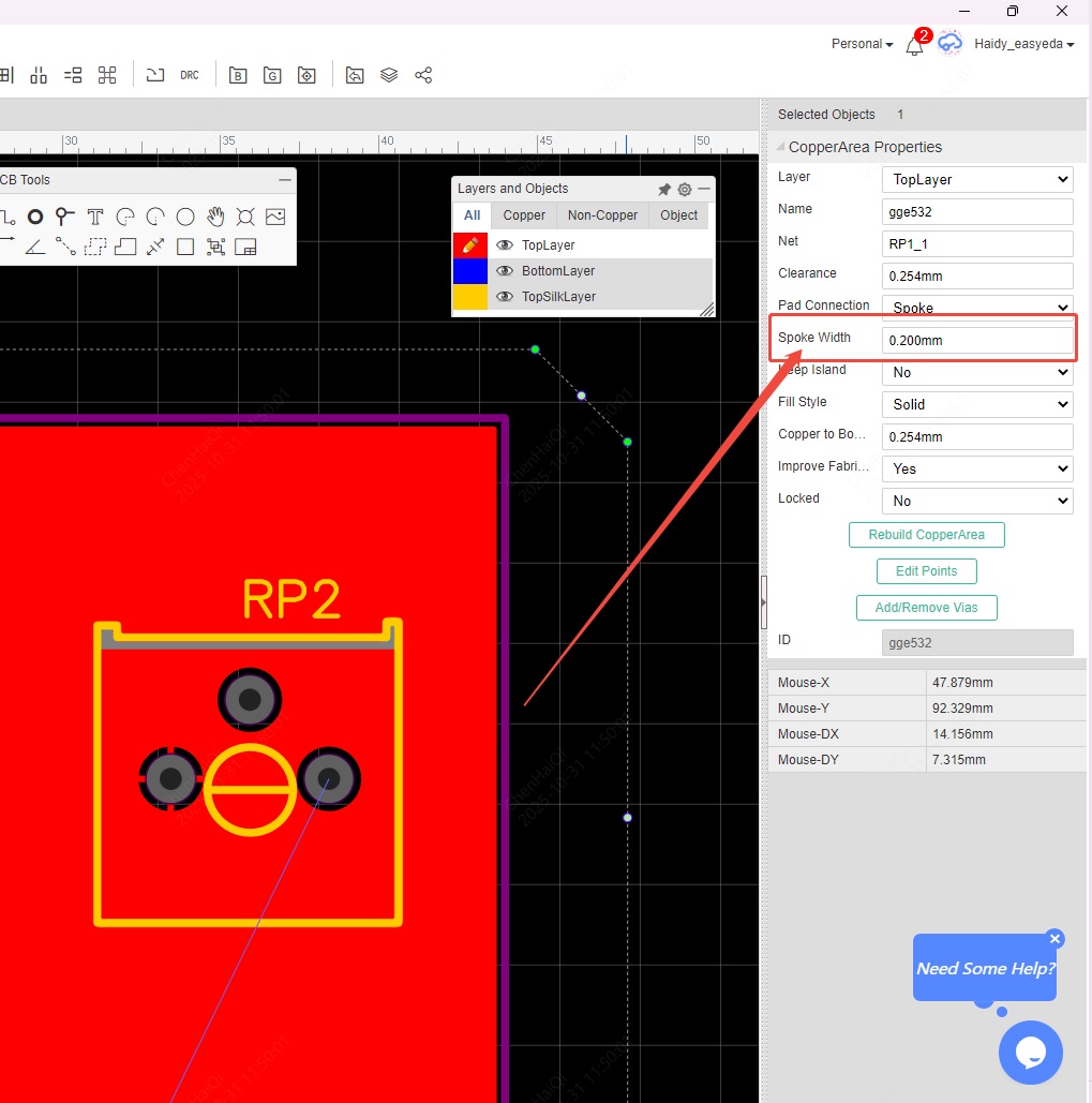
Spoke Width is generated when the connection method between the copper pour area and the pad is "spoke". The line width of the Spoke Width can be modified. 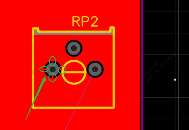
You can modify the copper pour area by clicking on it and looking at the properties panel on the right. 