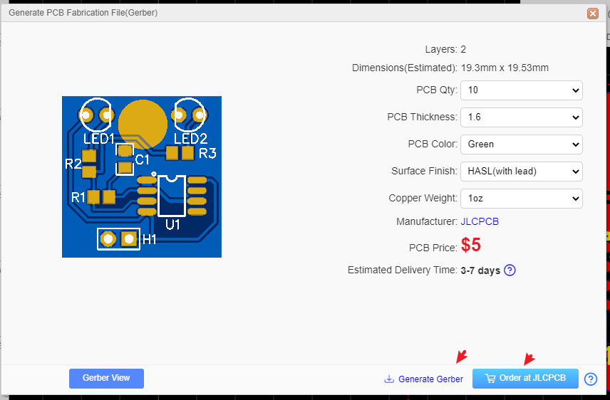
Generate Fabrication File(Gerber)
Generate Fabrication File Gerber
When you finish your PCB, you can output the Fabrication Files(gerber file) via: File > Generate PCB Fabrication File(Gerber) , or Fabrication > PCB Fabrication File(Gerber).

After clicking, will open the Gerber generate dialog:

You can calculate the price for the PCB order, click SAVE to CART will go to JLCPCB and add your PCB in the cart.
Gerber file name
The generated Gerber file is a compressed zip file. After decompression, you can see the following files:
| File Name | Type | Remarks/Description |
|---|---|---|
| Gerber_BoardOutline.GKO | Outline file | The PCB board factory cuts the board shape according to this file. The slots and solid-filled non-copper-plated through holes drawn by Jialichuang EDA are reflected in the border file after Gerber is generated. |
| Gerber_TopLayer.GTL | PCB Top Layer | Top Copper Foil Layer |
| Gerber_BottomLayer.GBL | PCB bottom layer | Bottom copper foil layer |
| Gerber_InnerLayer1.G1 | Inner copper foil layer, signal layer type. | |
| Gerber_InnerLayer2.GP2 | Inner copper foil layer, inner electrical layer type | |
| Gerber_TopSilkLayer.GTO | Top silkscreen layer | |
| Gerber_BottomSilkLayer.GBO* | Bottom silkscreen layer | |
| Gerber_TopSolderMaskLayer.GTS | Top Solder Mask Layer | It can also be called the window opening layer. By default, the board is covered with oil, and the elements drawn on this layer correspond to the area of the top layer, which is not covered with oil |
| Gerber_BottomSolderMaskLayer.GBS | Bottom Solder Mask | It can also be called the window layer. The board is covered with oil by default, and the elements drawn on this layer correspond to the area of the bottom layer without oil |
| Drill_PTH_Through.DRL | metallization drilling layer | This file shows the drill hole position that needs metallization on the inner wall, such as multi-layer pads, vias |
| Drill_PTH_Through_Via.DRL | via metallization drilling layer | This file shows the drill hole position that needs metallization on the inner wall, this file for JLCPCB use |
| Drill_NPTH_Through.DRL | Non-metallized drilling layer | This file shows the drill hole position that does not need metallization on the inner wall, such as through holes |
| Gerber_TopPasteMaskLayer.GTP | Top layer flux layer | For stencil opening |
| Gerber_BottomPasteMaskLayer.GBP | Bottom layer of soldering flux | For stencil opening |
| Gerber_TopAssemblyLayer.GTA | Top Assembly Layer | Only for reading, does not affect PCB manufacturing. Former name: ReadOnly.TopAssembly |
| Gerber_BottomAssemblyLayer.GBA | Bottom assembly layer | Only for reading, does not affect PCB manufacturing. Former name: ReadOnly.BottomAssembly |
| Gerber_MechanicalLayer.GME | Mechanical Layer | Only for reading, does not affect PCB manufacturing by default. Former name: ReadOnly.Mechanical. The information recorded in the mechanical layer in the PCB design is only for information recording. For example: process parameters, V-cut path, etc. |
| Gerber_DocumentLayer.GDL | Document Layer | Used to record PCB remarks, not involved in manufacturing |
Notice:
- Before ordering the PCB, please check the gerber at the Gerber view as below.
- The Gerber files are generated by browser, please use the browser inner downloader to download!
- The coordinates of the Gerber file follow the canvas coordinates
- When exporting Gerber, the drill file coordinate format accuracy defaults to 3:3. When the PCB size is out of range, it automatically uses 4:2 format. If you view the Gerber as such as CAM350, found that the Drill hole has been offset the location, you can modify the drill coordinate format to fit the location
Gerber View
Before sending Gerber to the factory, please use gerber viewer to check the Gerber carefully.
local gerber viewer you can use such as: Gerbv, FlatCAM, CAM350, ViewMate, GerberLogix etc.
Gerber viewer recommend Gerbv:
- Project page:http://gerbv.geda-project.org/
- Download: https://sourceforge.net/projects/gerbv/files/
How to use Gerbv:
1.Download Gerber zip file, and download Gerbv, unzip Gerber file and run the Gerbv;
2.Click the + button at the Gerbv dialog bottom-left corner, open the gerber folder, select all the gerber files, and open. 
3.And then zoom, measure, check every layer, check drill holes and location. etc.
FlatCAM is a nice tool too: http://flatcam.org/
FlatCAM lets you take your designs to a CNC router. You can open Gerber, Excellon or G-code, edit it or create from scatch, and output G-Code. Isolation routing is one of many tasks that FlatCAM is perfect for. It's is open source, written in Python and runs smoothly on most platforms.
Free Online Gerber Viewer:
Recommend: https://dfm.jlcpcb.com/