Shortcut Keys
While using an EDA tool suite, clicking all over the place with a mouse can get very tedious and seriously reduces your productivity. Keyboard shortcuts or Hotkeys avoid much of that. EasyEDA not only provides many hotkeys, but also every hotkey can be reconfigured to your personal preference.
Under the Setting menu, click the Hotkeys Setting... Menu which will open the Hotkey Setting dialog. 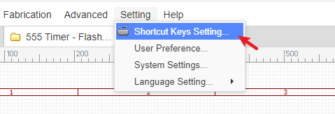
To change a Hotkey, click anywhere in the row for the hotkey you want to change and then press your new key.
For example, if you want to use R instead of space to rotate selected objects, click on the first row, then press R.
After changing any hotkey, you must click the Save Changes button.
The docType column describes which type of EasyEDA document each hotkey applies to. docType has three types:
- ALL: any document type in EasyEDA.
- SCH: schematic and schematic libs
- PCB: PCB and Footprints.
The functions of some hotkeys may change between docTypes. For example, the hotkey C draws an Arc in SCH but draws a circle in PCB.
A list of all the available default hotkeys is given below.
All document
| DocType | Shortcut | Function |
|---|---|---|
| All | Space | Rotate selected objects |
| All | Right-Click | Keep right-click to pan canvas; Open offset dialog when select one object |
| All | Left | Scroll Or Move selected left |
| All | Right | Scroll or Move selected right |
| All | Up | Scroll or Move selected up |
| All | Down | Scroll or Move selected down |
| All | TAB | Change object's attributes when placing; Open offset dialog when selecting an object |
| All | Esc | Cancel current drawing |
| All | Home | setting new canvas origin |
| All | Delete | Delete Selected |
| All | F1 | Open tutorials |
| All | F11 | Full screen at browser |
| All | A | Zoom In |
| All | Z | Zoom Out |
| All | D | Drag |
| All | K | Fit Window |
| All | R | Rotate selected objects |
| All | X | Flip Horizontal(doesn't support footprint) |
| All | Y | Flip Vertical(doesn't support footprint) |
| All | ALT+F5 | Full screen at browser |
| All | ALT+W | Close current tab |
| All | SHIFT+ALT+W | Close all tabs |
| All | CTRL+X | Cut |
| All | CTRL+C | Copy |
| All | CTRL+V | Paste |
| All | CTRL+A | Select All |
| All | CTRL+Z | Undo |
| All | CTRL+Y | Redo |
| All | CTRL+S | Save |
| All | CTRL+F | Find Component |
| All | CTRL+D | Design Manager |
| All | CTRL+Home | Open canvas origin setting dialog |
| All | SHIFT+1 | Cycle forward to next open tabbed document |
| All | SHIFT+2 | Cycle backward to next open tabbed document |
| All | SHIFT+X | Cross Probe |
| All | SHIFT+F | Search Library |
| All | SHIFT+Drag | Cursor snap to part's origin |
| All | SHIFT+ALT+H | Align horizontal centers |
| All | SHIFT+ALT+E | Align verticas centers |
| All | CTRL+SHIFT+L | Align left |
| All | CTRL+SHIFT+R | Align right |
| All | CTRL+SHIFT+O | Align top |
| All | CTRL+SHIFT+B | Align bottom |
| All | CTRL+SHIFT+G | Align grid |
| All | CTRL+SHIFT+H | Distribute Horizontally |
| All | CTRL+SHIFT+E | Distribute Vertically |
| All | CTRL+SHIFT+F | Find similar objects |
Schematic
| DocType | Shortcut | Function |
|---|---|---|
| Schematic | W | Draw Wire |
| Schematic | B | Draw Bus |
| Schematic | U | Bus Entry |
| Schematic | N | NetLabel |
| Schematic | P | Place Pin |
| Schematic | L | Draw Polyline |
| Schematic | O | Draw Polygon |
| Schematic | Q | Draw Bezier |
| Schematic | C | Draw Arc |
| Schematic | S | Draw Rect |
| Schematic | E | Draw Ellipse |
| Schematic | F | Freehand Draw |
| Schematic | T | Place Text |
| Schematic | I | Edit Selected Symbol |
| Schematic | CTRL+Q | NetFlag VCC |
| Schematic | CTRL+G | NetFlag GND |
| Schematic | F8 | Run the Document Simulation |
| Schematic | CTRL+J | Open the Simulation Setting |
| Schematic | CTRL+SHIFT+X | Cross Probe and Place |
| Schematic | SHIFT+T | Open symbol wizard |
| Schematic | ALT+F | Open footprint manager |
PCB
| DocType | Shortcut | Function |
|---|---|---|
| PCB | W | Draw Track |
| PCB | U | Draw Arc |
| PCB | C | Draw Circle |
| PCB | N | Draw Dimension |
| PCB | S | Draw Text |
| PCB | O | Draw Connect |
| PCB | E | Draw copperArea |
| PCB | T | Change To TopLayer; Change selected part to toplayer |
| PCB | B | Change To BottomLayer; Change selected part to bottomlayer |
| PCB | 1 | Change To Inner1 |
| PCB | 2 | Change To Inner2 |
| PCB | 3 | Change To Inner3 |
| PCB | 4 | Change To Inner4 |
| PCB | P | Place Pad |
| PCB | Q | Change canvas unit |
| PCB | V | Place Via |
| PCB | M | Measure |
| PCB | H | Highlight Net all the time, press it again cancel highlight |
| PCB | L | Change Route Angle |
| PCB | - | Decrease Routing Width; Switch to the forward signal layer |
| PCB | + | Increase Routing Width; Switch to the next signal layer |
| PCB | * | Cycle switch to the next signal layer |
| PCB | Delete | Delete selected object; Undo the track when routing |
| PCB | ALT-- | Decrease Snap Size |
| PCB | ALT++ | Increase Snap Size |
| PCB | CTRL+R | Depend on reference point for copy object repeatly |
| PCB | CTRL+L | Open layer manager |
| PCB | CTRL+Q | Hide/show network text |
| PCB | SHIFT+M | Remove All Copper Area fill data |
| PCB | SHIFT+B | Rebuild All Copper Area |
| PCB | SHIFT+D | Move Object(s) by reference point |
| PCB | SHIFT+G | Display track length while routing |
| PCB | SHIFT+W | Show favorite track width while routing |
| PCB | SHIFT+R | Change routing conflict |
| PCB | SHIFT+S | Toggle layers which is not active |
| PCB | SHIFT+Double Click | Delete selected track segment |
| PCB | CTRL+SHIFT+V | Paste object(s) and keep the prefix, and hide the ratline layer |
| PCB | CTRL+SHIFT+SPACE | Change routing angle, same as hotkey L |
| PCB | CTRL+ALT+L | Enable all layers |
| Footprint | CTRL+SHIFT+ALT+D | Open custom data dialog |