PCB Layout
When you are satisfied with your schematic design and simulation results, you can then quickly proceed to produce your finished and populated PCB without leaving EasyEDA.
EasyEDA's PCB Design canvas helps you to quickly and easily lay out even complex multilayer designs from schematics you have already created in the Schematic canvas or directly as a layout with no schematic.
Passing an EasyEDA Schematic into the PCB Design editor is as easy as clicking a button: Just click the Convert to PCB using: "Menu - Design - Convert to PCB".

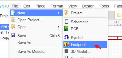
EasyEDA has extensive component footprints. You can also build up your own library of unusual and specialized parts by copying and modifying existing parts or from scratch using EasyEDA’s powerful footprint creation and editing tools.
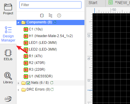
When working in the PCB Design canvas there is a PCB Design Manager which works in a similar way to the Schematic design canvas, this will help you locate items and navigate your way around. Left Navigation Panel > Design Manager The PCB Design Manager is a powerful tool for finding components, tracks (nets) and pads (Net Pads). Clicking on any item highlights the component and pans it to the center of the window.
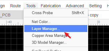
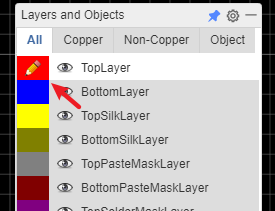
You can set up layers used in the PCB and their display colours and visibility using Top Menu - Tools - Layer Manager...
 The active layer and layer visibility can be selected using the Layers Toolbar.
Default track widths, clearances and via hole dimensions can all be configured in the Design Rule Check dialog which is opened by: Top Menu > Design > Design Rule...
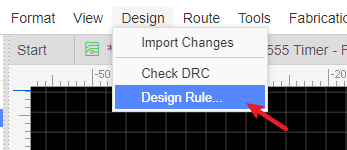 The Design Rule Check (DRC) is created when beginning your board layout. It can also be modified at any time. Running a DRC is one of the last steps in checking your PCB design before you generate Gerber and Drill files for board manufacture and are ready to place your order for a finished PCB.
The final step is to check the Gerber and Drill files using a software Gerber viewer. This is an easy to install and use Open Source Software Gerber Viewer: Gerbv: http://gerbv.geda-project.org/
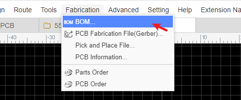
While you are waiting for your PCB to be delivered or at any time it is needed, you can create a Bill of Materials (BOM) with: File > Export BOM... or Top Menu - Fabrication - BOM...
You can produce professional quality
SVG,.pngor.pdfoutput files for your documentation.
PCB Designs can be shared with colleagues and made public in the same way as Schematics. The size of PCB that you can produce using EasyEDA is almost unlimited: designs of over 100cm * 100cm are possible … but you might need a powerful computer for that.
EasyEDA supports up to 6 layer PCBs by default but it is capable of handling more, so if you need more layers then please contact us.
Search footprints
Searching footprints is the same as searching symbols by using Library in the Schematic editor. You can place the selected footprints in the canvas after a successful search.